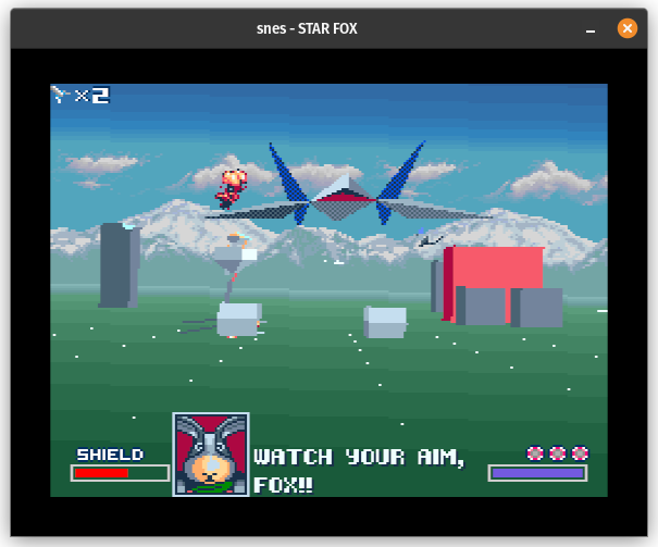
The Super FX chip is easily the most well-known SNES coprocessor, primarily because of Star Fox which renders real-time 3D graphics on the SNES with the help of the Super FX. Yoshi’s Island also uses the Super FX, though mainly for sprite scaling/rotation and various graphical effects rather than 3D rendering.
So how does it work?
Overview
The core component inside the Super FX is the Graphics Support Unit, or the GSU. The GSU is a 16-bit RISC CPU that was custom-designed by Argonaut Games specifically to use in Star Fox.
In addition to the GSU, all Super FX cartridges include either 32KB or 64KB of RAM that is accessible to both the GSU and the SNES CPU (though not simultaneously).
The most unique aspect of the GSU is that it has a set of bitmap plotting instructions. Software running on the GSU can draw bitmap graphics into an on-chip pixel buffer, and the chip has specialized graphics conversion hardware that will automatically convert the plotted bitmap graphics to the SNES bitplane graphics format as it flushes the pixel buffer into RAM. Once a scene is complete, the SNES CPU can kick off a DMA to copy the rendered scene directly from Super FX cartridge RAM to VRAM.
These plotting instructions combined with the GSU having fairly fast multiplication instructions make it possible to write a software renderer that can render basic 3D graphics in real-time. There is no real 3D graphics acceleration hardware here - only hardware that makes it possible to efficiently plot pixels in the SNES graphics format. All of the actual 3D rendering is implemented in software that runs on the GSU.
RISC
RISC, or reduced instruction set computer, refers to CPUs that have a simplified instruction set designed to be more efficient to implement in hardware as well as easier for compilers to target. Using the classical definitions, the primary difference between RISC and CISC (complex instruction set computer) is that RISC CPUs typically have dedicated load/store instructions for accessing memory while CISC CPUs typically allow many instructions to access memory using different addressing modes. RISC CPUs also nearly always have fixed-length opcodes, while CISC CPUs may have variable-length opcodes. (It’s worth noting that CISC is not very well defined and really just means “not RISC”.)
For example, in a RISC CPU, the ADD instruction can only read from CPU registers and write to CPU registers. Explicit load and store instructions are needed to read an operand from memory or write the result to memory. In a CISC CPU, the ADD instruction might support a number of different addressing modes for reading the operand: read from a register, read from an absolute memory address, read from an indexed memory address, etc.
The main benefit of simplifying the instruction set like this is that it makes pipelined execution much, much easier to implement in hardware. Early CISC CPUs can only execute one instruction at a time, maybe with some fetch/execute overlap. RISC CPUs can break instructions into multiple stages and can easily execute multiple instructions simultaneously as long as each instruction is in a different stage. Many RISC CPUs can execute most instructions in a single clock cycle from software’s perspective as long as there are no delays caused by memory accesses or extra-long instructions (e.g. long multiplication in the Super FX GSU).
RISC CPUs will often avoid storing additional operands in opcodes because that causes operand reading to stall the pipeline, but the Super FX GSU actually does this. Specifically, some of the RAM load/store instructions put the RAM address in the 1-2 opcodes following the instruction opcode.
The downside to RISC is that programs often require more instructions compared to an equivalent CISC program, and writing raw assembly for a RISC CPU can be more tedious in some cases.
Chip Variants
There are 3 different variants of the Super FX chip that were used in actual cartridges. The first variant is called the Mario Chip, supposedly a backronym from “Mathematical, Argonaut, Rotation, and Input/Output”. The two later variants are called the GSU-1 and the GSU-2. All three variants have the exact same functionality, but the GSU-1 and GSU-2 support higher clock speeds than the Mario Chip, and the GSU-2 also supports additional cartridge memory.
The GSU can run at a clock speed of either 10.74 MHz (SNES mclk/2) or 21.47 MHz (SNES mclk/1). Mario Chip only supports 10 MHz while GSU-1 and GSU-2 support both speeds.
It’s believed that the Mario Chip and the GSU-1 only support up to 1MB of ROM while the GSU-2 supports up to 2MB. The GSU-2 also has connections for additional ROM/RAM that would have been accessible to the SNES CPU while the GSU is running, but none of the released GSU-2 games used those connections.
Here is the breakdown of which Super FX games used which chip:
- Mario Chip: Star Fox
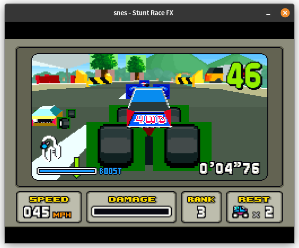
- GSU-1: Stunt Race FX, Dirt Trax FX, Dirt Racer, Vortex
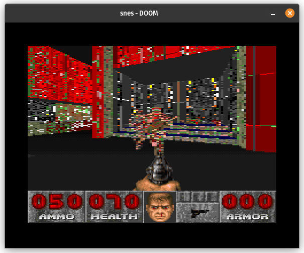
- GSU-2: Yoshi’s Island, Doom, Winter Gold
The (originally) unreleased Star Fox 2 almost certainly would have used GSU-2.
SNES Coordination
GSU execution flow is similar to the DSP inside the Cx4 coprocessor.
Normally the GSU is idle. When the SNES CPU wants it to execute a routine, it configures the GSU by writing to memory-mapped registers, and then it writes to the GSU’s program counter register which initiates GSU execution. Once the GSU starts running, it continues until it executes a STOP opcode which halts it until the SNES CPU starts it up again. The SNES CPU can poll a status register to see whether the GSU is running or halted.
The SNES CPU can also start the GSU by setting the GO=1 bit in the GSU’s status register, which causes the GSU to resume execution wherever it stopped.
Access to the cartridge bus is mutually exclusive between the SNES CPU and the GSU. While the GSU is running, the SNES CPU controls whether it or the GSU owns the cartridge bus. If the GSU owns the bus, SNES CPU writes to cartridge RAM will do nothing and reads from ROM/RAM will return a fixed value based on the last 4 bits of the address (meant to be 65816 interrupt vectors in case an interrupt triggers while the GSU is running). If the SNES CPU owns the bus, the GSU will stall if it accesses ROM or RAM, and it will remain stalled until the SNES CPU gives the bus back to the GSU.
GSU routines almost always write their output into Super FX cartridge RAM. Once the GSU is finished, the SNES CPU can read the result directly out of cartridge RAM, usually via DMA. Graphical output will be in the SNES bitplane format so that the SNES can DMA it directly from cartridge RAM to VRAM.
Graphics Support Unit
Rather than cover the entire instruction set, I’ll cover the parts that are somewhat or very unique.
General
The GSU has 16 mostly general-purpose 16-bit registers that can be used as operands with any of the ALU instructions. The main exceptions are:
R0 is fixed to zero; reads always return 0 and writes do nothingEDIT: This is incorrect, I was thinking of the PS1’s CPU when I wrote this.- R14 is the current ROM pointer; writing to this register triggers a ROM buffer reload (more on that later)
- R15 is the current program counter, automatically incremented as the GSU fetches opcodes
A number of the other registers have special uses with specific instructions, but they are general-purpose when used with other instructions. Note that executing an instruction that writes to R15 is functionally equivalent to a jump, though the GSU does also have dedicated jump opcodes that are slightly faster.
Much like the 65816, the GSU has an 8-bit PBR (program bank register) alongside the 16-bit program counter. GSU code can only modify the PBR using an LJMP instruction, which changes both PBR and R15.
All opcodes are fixed-length 8-bit, but a number of opcodes are prefix opcodes that modify the next non-prefix instruction instead of doing anything themselves. These modifications include:
- ALT1/ALT2/ALT3: Execute different variants of the same basic instruction (e.g. ADD vs. ADC, or immediate operand vs. register operand)
- FROM/TO/WITH: Specify register operands for instructions that can’t embed the register number(s) in the opcode
- WITH additionally specifies that an immediately following FROM or TO should perform a register-to-register load operation instead of being treated as a prefix
Because instruction execution is pipelined, the GSU has what are called branch delays or branch hazards. Basically, when a jump or branch is taken, the CPU has already started to execute the instruction immediately following the jump/branch instruction. It would be expensive to cancel this mid-instruction so it simply doesn’t. For the GSU (and many other older RISC CPUs), this is considered normal behavior - the instruction after a jump/branch will always be executed, even if the branch is taken. Games do depend on this as they’ll typically try to do something useful in that instruction slot, which is often called the branch delay slot.
Note that branch delays also affect the STOP instruction. The GSU will always execute the instruction after the STOP before it halts. If the SNES CPU then starts the GSU again without changing R15 (which it can do by writing GO=1 in the status/flags register), the GSU will start execution from the instruction two past the STOP instead of the one immediately after the STOP.
Code Cache
While the GSU hardware is capable of executing ~21 million basic ALU instructions per second, cartridge memory isn’t capable of responding quickly enough to support that. Every ROM or RAM access normally takes 3 cycles in 10 MHz mode and 5 cycles in 21 MHz mode. On paper, this heavily slows down the GSU since it needs to access ROM or RAM at least once per instruction for the opcode read.
To work around this limitation, the GSU has 512 bytes of very fast code cache RAM. If the next opcode to be executed is found in code cache, the GSU can read it out of cache instead of needing to fetch from slow memory. For the basic ALU instructions, this means the instruction taking 1 cycle instead of 3/5 cycles.
Some CPUs make code cache completely transparent to software, but the GSU does not. Software is responsible for managing the code cache location.
The GSU has a 12-bit register called CBR (cache bank register) that specifies the starting address of the 512-address block that should be covered by code cache. Opcode fetches from addresses in that block will use code cache if the address hits in the cache, and otherwise the read will automatically populate the cache after fetching from ROM/RAM. Opcode fetches from addresses outside of the covered 512-address range will ignore the code cache and will always fetch from ROM/RAM.
Software’s primary tool for managing code cache is the CACHE instruction, which fully invalidates the cache and changes CBR to point to the instruction following the CACHE instruction (aligned to a 16-byte boundary since CBR is 12-bit). Typically, software will put a CACHE instruction at the start of a loop that will be executed many times, and ideally all routines called by the loop will be located within the 512 bytes following the CACHE instruction. The first execution of the loop will populate the code cache, and successive executions will execute fully out of code cache which will be many times faster than executing out of ROM or RAM.
Executing an LJMP instruction also invalidates the cache (and changes CBR), just in case the software is about to start executing from cache-covered addresses in a different program bank.
Some documentation refers to a mode of GSU execution where the SNES CPU manually populates code cache RAM with a GSU routine prior to starting the GSU, and then once started the GSU will execute entirely out of code cache without ever accessing ROM or RAM. While this is technically possible to do, I don’t believe any of the released Super FX games do this. It has rather limited utility since there’s not much useful that the GSU can do without ever writing to RAM.
Buffers
In order to speed up GSU execution in common use cases, ROM reads and RAM writes are typically asynchronous. The GSU manages this using a ROM read buffer and a RAM write buffer. (Opcode reads are an exception - opcode reads from ROM are always synchronous.)
ROM
The ROM read buffer is reloaded any time the GSU writes to R14, the ROM pointer register. Every write to R14 triggers an asynchronous ROM read from the 16-bit address specified by R14 in the current 8-bit data ROM bank (set using the ROMB instruction).
The GSU has dedicated instructions for reading data from ROM: GETB, GETBL, GETBH, GETBS, and GETC. Each of these instructions reads its input from the ROM buffer instead of directly accessing ROM. If a ROM buffer read is currently in-progress, the instruction will block until the ROM buffer read completes. Software can take advantage of this by writing to R14 to trigger a ROM buffer reload, executing several other useful instructions, and then executing the instruction that uses the ROM data so that it will not have to wait for it.
One quirk with the ROM buffer is that changing the data ROM bank does not trigger a ROM buffer reload, and Doom depends on this! It executes GETC instructions following ROMB instructions, and it expects the GETC to return a ROM byte from the previous ROM bank instead of the new bank. If GETC returns a byte from the new ROM bank then the game will look like this:
RAM
Similar to ROM, the GSU has dedicated instructions for accessing RAM:
- Read: LDB, LDW, LM, LMS
- Write: STB, STW, SM, SMS, SBK
Writes to RAM pass through a RAM write buffer. If the GSU executes a RAM write while the buffer is empty, the GSU can simply put the write in the buffer and then write to RAM asynchronously while instruction execution continues. If a RAM write is already in-progress then the instruction will block until it can put the write in the buffer. Programs that are doing more than bulk writing to RAM can take advantage of this by spacing out RAM write instructions.
The GSU also remembers the last RAM address that was read from using a load instruction, specifically for the SBK instruction which writes to that memorized RAM address. This is faster than using one of the other store instructions if a program wants to read a value from RAM, do something with it, and then write a new value back to that same address.
RAM reads are not buffered and must always wait for RAM to return the requested value.
It’s somewhat unclear what happens if the GSU reads from RAM while an asynchronous RAM write is in-progress. Opcode reads from RAM appear to block during an in-progress RAM write, but LDB/LDW/LM/LMS reads possibly do not block?
Plotting Instructions
Now for what makes the GSU really unique, and what justifies its name as Graphics Support Unit.
It’s probably easiest to start with how the GSU draws graphics from software’s perspective.
PLOT
Logically, the PLOT instruction plots a pixel color to specific X and Y coordinates that are specified in registers (R1 = X, R2 = Y). The pixel color is set beforehand using either a COLOR instruction (set color from a general-purpose register) or a GETC instruction (set color from the ROM buffer).
X and Y coordinates into what, you might be asking?
The Super FX chip maintains a “virtual screen” in RAM (essentially a frame buffer) that is sized at either 256x128px, 256x160px, or 256x192px. There is also an “OBJ mode” setting meant for sprite drawing that splits the virtual screen into a 2x2 grid of smaller screens that are each 128x128px.
The X and Y parameters to the PLOT instruction are pixel coordinates into that virtual screen. The virtual screen is always stored in RAM in the SNES bitplane format, and this is where the magic happens.
The GSU maintains an 8-pixel-wide pixel buffer in bitmap format, which is very convenient for software rendering. Software can configure the GSU’s color depth to be 2bpp (4-color), 4bpp (16-color), or 8bpp (256-color) by having the SNES CPU write to the SCMR (screen mode) register, which also configures the virtual screen size.
When software executes a PLOT instruction, the GSU normally just writes the color value into the pixel buffer and then continues instruction execution. When the pixel buffer needs to be flushed for any reason, the Super FX hardware automatically converts the bitmap pixels in the buffer into the SNES bitplane format and then writes them out to the virtual screen in RAM. It uses the current virtual screen size configuration combined with the buffer’s X/Y coordinates to determine the RAM addresses to write to.
The pixel buffer is flushed when any of the following happens:
- All 8 pixels in the buffer have been written since the last flush
- PLOT is executed with Y or (X / 8) different from the last PLOT call, and there was at least 1 pixel written since the last flush
- Software executes an RPIX instruction (read pixel), which synchronously flushes the pixel buffer before performing its read
The Super FX chip keeps track of which pixels in the buffer have been written since the last flush. If it performs a flush when not all 8 have been written, the chip will automatically read existing pixel data from RAM and merge it with the pixel buffer before writing to RAM (though this does have a performance cost). This is to ensure that it only overwrites bits for pixels that have actually been plotted.
There are technically two pixel buffers, a primary buffer and a secondary buffer, but that detail isn’t really important for emulation except for emulating flush timings. PLOT instructions write into the primary buffer. The primary buffer is flushed by simply copying the contents into the secondary buffer, and then the GSU begins to asynchronously write to RAM from the secondary buffer. The GSU can continue writing into the primary buffer using PLOT instructions while a secondary buffer RAM write is in progress, but if the primary buffer needs to be flushed then the GSU will block until the RAM write finishes.
RPIX is sort of exceptional in that in addition to forcing a primary buffer flush, it will always block until any in-progress RAM write is complete to ensure that it doesn’t read stale pixel data from RAM. Software often executes RPIX right before terminating the GSU to guarantee that the pixel buffer is completely flushed out to RAM. Using RPIX to actually read pixel data is rare because it’s an extremely slow instruction (minimum ~24 cycles according to documentation), but Yoshi’s Island has several effects that do depend on emulating RPIX read behavior correctly.
Virtual Screen Mapping
The main trick behind Super FX is the hardware that manages the virtual screen in RAM.
The virtual screen base address, the size, and the color depth (2bpp/4bpp/8bpp) are configurable by software. Using 2bpp and 256x192 as an example, the pixel buffer flush to RAM works roughly like this:
|
|
4bpp and 8bpp work similarly only with different tile sizes and writing 4/8 bitplanes instead of 2.
256x128 and 256x160 screen sizes work pretty much the same only with a different number of tiles per row in the virtual screen. OBJ mode works a little differently - the highest bit of X and Y are used to determine which of the 4 smaller screens in the 2x2 screen grid to use, and then the remaining 7 bits in each are used as a pixel position within the 128x128 smaller screen.
CMODE
Software can use the CMODE instruction to customize a few plotting options. These are:
- Force OBJ mode: Causes the GSU to ignore the configured virtual screen size and always use OBJ mode
- This is mainly useful because the GSU can’t change the screen size itself - only the SNES CPU can
- Dithering: In PLOT instructions, if X ^ Y is odd then the GSU will plot
color >> 4instead of plottingcolor- This is only really useful in 2bpp or 4bpp mode, where each nibble can store a different 2bpp/4bpp color value. The GSU will alternate between the two color values to produce a dithered pattern
- Freeze high nibble: Prevents COLOR and GETC instructions from changing the highest 4 color bits
- High nibble flag: Causes COLOR and GETC instructions to duplicate the high nibble into the low nibble on writes, ignoring the lowest 4 bits written
- Plot transparent pixels: Normally, PLOT does not write transparent pixels (color == 0) to the pixel buffer; this flag causes them to be written
One note with transparent pixels is that the GSU only checks the lowest N bits to determine transparency, where N is the configured color depth in bits (2/4/8). There is also a quirky interaction with the freeze high nibble flag: If the freeze high nibble flag is set while in 8bpp mode, the GSU will only check the lowest 4 bits to determine transparency instead of checking all 8. Stunt Race FX depends on emulating this correctly or some graphics will have a solid color drawn where there should be transparency:
Memory Map
The Super FX memory map is pretty simple, although the SNES CPU and the GSU do each get their own memory map.
All Super FX cartridges have at most 2MB of ROM and either 32KB or 64KB of RAM. Roughly half of the Super FX games have battery backups for RAM: Yoshi’s Island, Star Fox 2, Stunt Race FX, and Winter Gold.
SNES CPU
ROM is mapped in both LoROM and HiROM mappings, similar to SA-1. $8000-$FFFF in banks $00-$3F + $80-$BF contains a LoROM mapping for ROM, while $0000-$FFFF in banks $40-$5F + $C0-$DF contains a HiROM mapping for ROM.
The first 8KB of RAM is mapped to $6000-$7FFF in the I/O area banks, similar to standard HiROM cartridges. The full 32-64KB of RAM is mapped to banks $70-$71 and $F0-$F1.
The GSU’s 512 bytes of code cache RAM are mapped to $3100-$32FF in the I/O area banks, but I don’t think any of the Super FX games access code cache directly from the SNES CPU. There are some test ROMs that exercise this mapping though, as well as the behavior that GSU will execute entirely out of code cache if the SNES CPU manually populates it before starting the GSU.
The mapping from $3100-$32FF addresses to code cache addresses is a bit weird because $3100 is not necessarily the beginning of the code cache - it depends on the lowest bits of the CBR. If the code cache starts at $9FC0 for example, addresses are offset so that $32C0 (0x3100 + (0x9FC0 & 0x01FF)) would map to the beginning of code cache:
|
|
I don’t believe any games depend on this since it would be quite strange for the SNES CPU to access code cache RAM while the CBR is not 0. The SNES CPU can’t explicitly set the CBR - it can only reset it to 0 by writing GO=0 to the GSU status register.
Super FX registers are mapped to $3000-$30FF and $3300-$34FF in the I/O area banks, but games should generally only access them through $3000-$303F addresses. All accesses are masked with $3F.
GSU
The GSU memory map is pretty similar to the SNES CPU’s memory map, only without the direct mappings for code cache and the Super FX registers. GSU software also never seems to access banks $80-$FF - it’s unclear whether they mirror banks $00-$7F.
ROM is mapped to banks $00-$3F with LoROM mapping and to banks $40-$5F with HiROM mapping. In banks $00-$3F, $0000-$7FFF mirrors $8000-$FFFF since the GSU doesn’t have an I/O area.
RAM is mapped to banks $70-$71.
The GSU can’t directly access code cache RAM, but it will populate and use code cache when fetching opcodes from addresses that are covered by code cache. Some documentation claims that $0000-$01FF is specially mapped to code cache RAM for opcode fetches but I don’t think that’s right - that just happens to be the range of addresses covered by code cache with the default code cache location (CBR=0).
Sega Virtua Processor
As an aside, the sole Sega Genesis coprocessor was very clearly inspired by the Super FX.
Only one Genesis game used a coprocessor (at least during the console’s normal lifetime): the Genesis port of Virtua Racing, which released roughly a year after Star Fox. This coprocessor is called the Sega Virtua Processor, or SVP for short. Sega originally had plans to use the SVP in other games, but Sega being Sega they instead decided to abandon the standalone Genesis to focus on the 32X and later the Saturn. Oh well.
Similar to Star Fox and the Super FX, Virtua Racing uses the SVP to render 3D graphics in real time on the Genesis:
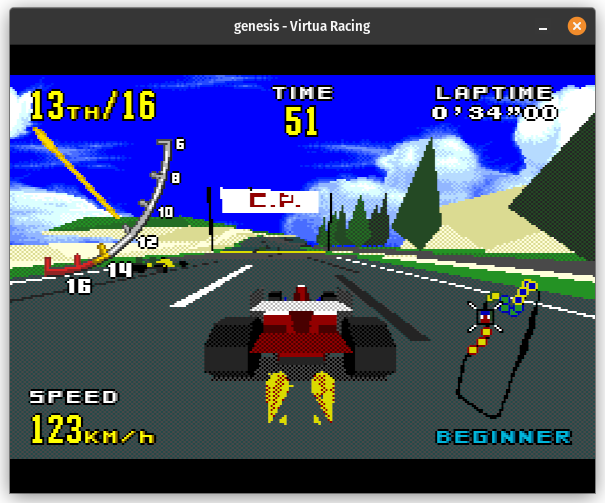
The idea is pretty similar to Super FX though without the graphical conversion hardware. The SVP contains a Samsung SSP1601 DSP that is capable of very fast (for the time) multiplication and multiply-accumulate operations, and the cartridge ROM contains a software renderer program that runs on the DSP. The DSP program renders 3D scenes into cartridge RAM, and then the Genesis CPU kicks off a DMA that copies the rendered 3D scenes from cartridge RAM to VRAM.
The graphical conversion hardware was probably less necessary on the Genesis because the Genesis VDP’s packed pixel graphics format is significantly easier for a software renderer to work with than the SNES PPU’s bitplane graphics format. Where the SNES format spreads the bits for a pixel across 2/4/8 different bytes, the Genesis format puts of all of a pixel’s bits into the same byte, packing together 2 pixels per byte.
This version of Virtua Racing is really only a curiosity nowadays, as it was largely obsoleted by the superior 32X port and it was never as good as the arcade original.
Conclusion
The key thing that makes Super FX work is the plotting instruction set that allows software to draw graphics into a logical bitmap while specialized hardware deals with converting the plotted graphics from bitmap format to the SNES graphics format. This made it possible to write software renderers capable of drawing 3D graphics in real time on the SNES, which was incredible back in 1993. Super FX is the most well-known SNES coprocessor because its games are easily the most technically impressive out of all of the coprocessor games.
Super FX games do tend to suffer from rather low framerates. An emulator can solve this with an option to overclock the GSU compared to actual hardware, although this causes some of the games to just run faster since the game speed is not always decoupled from the framerate. Winter Gold also seems to be very sensitive to the GSU running too fast and will have glitchy player graphics when run with an overclocked GSU.
Anyway, that’s the last SNES coprocessor! Well, except for ST018, which I didn’t cover in detail because I haven’t emulated it and I don’t plan to.