SPC7110 is a data decompression chip very similar to S-DD1, but it also has a number of other features that games make use of, with one of the three SPC7110 games even including a real-time clock chip on the cartridge.
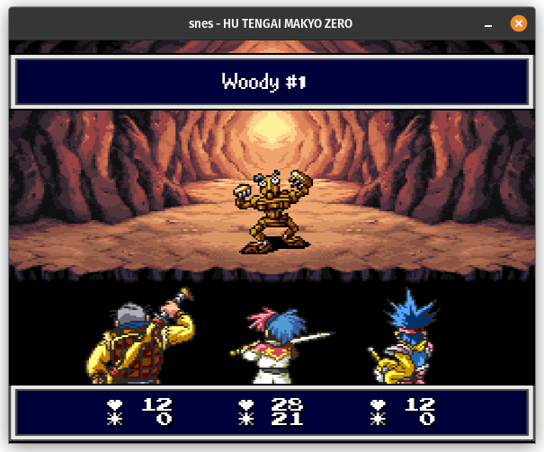
This chip was used in 3 games, all Japan-only games by Hudson: Tengai Makyou Zero, Momotarou Dentetsu Happy, and Super Power League 4. Tengai Makyou Zero is by far the most well-known of these - it’s a prequel to the Tengai Makyou series of RPGs on the PC Engine CD. While Tengai Makyou is hardly known outside of Japan, Tengai Makyou 2 regularly shows up on best-game-of-all-time lists from Japanese gamers.
For a long time Tengai Makyou Zero was only playable in Japanese, but it got a complete English fan translation in 2017.
Decompression Algorithm
I’m not going to go fully in-depth here like I did with S-DD1 because the algorithm is somewhat similar to S-DD1’s, and also because I frankly don’t understand the SPC7110 algorithm as well. nocash’s fullsnes documentation has pseudocode that implements the algorithm, and there is also this NESDev thread where the SPC7110 algorithm was reverse engineered, but I couldn’t find an equivalent of the S-DD1 wiki page on the SFC Development wiki.
Encoding
SPC7110 uses an adaptive compression algorithm with a context model specialized for SNES tile data, much like S-DD1, but the details of how it works are rather different. Like S-DD1, SPC7110 maintains the current MPS value and the current state for each context. Unlike S-DD1, there’s only one decoder, and it works very differently from S-DD1’s decoder.
Rather than directly encoding run lengths like S-DD1 does, SPC7110 uses a form of arithmetic coding, where the raw bitstream is compressed into what is essentially an extremely long decimal number between 0 and 1. The decoder keeps track of the probability of MPS vs. LPS at all times, and it uses that with an 8-bit counter called TOP in order to decode the number into decompressed bits. The coding algorithm is designed such that when the MPS probability is very high, MPS runs can be encoded using very few bits while an LPS takes many more bits to encode. When the MPS and LPS probabilities are close to 50%, MPS and LPS encoding take roughly the same number of bits.
This page from the NESDev thread has some useful discussions and links for understanding the encoding.
TOP is an 8-bit counter in hardware, but logically it represents a value between 1 and 256. Treating it as a 1-256 value, the basic decoding loop is:
|
|
The SPC7110 decoder has 53 different states, with the following per-state probability values:
|
|
These are the next state tables:
|
|
Essentially, MPS state transitions move the decoder to a higher state within one of these 5 groups (and potentially to a lower group), while LPS state transitions move the decoder to a higher group. Higher states within a group have a lower LPS probability, and lower groups have the LPS probability decrease more rapidly as the decoder goes through MPS state transitions.
Decoding a single bit in greater detail looks roughly like this:
|
|
Context Model
Like S-DD1, SPC7110 stores a separate MPS value and current state for each context, but the way SPC7110 determines the context is much more complex.
There are 3 different context model modes: one for 2bpp tile data (mode 1), one for 4bpp tile data (mode 2), and one for other data (mode 0). They each use the same decoding algorithm with a different context model.
To be blunt, I do not understand this part of SPC7110 well at all and so I don’t think there’s much value in me attempting to explain it. All three context model modes do factor in previous bits in the decompressed bitstream in order to compute the context for the next bit, but the details regarding how exactly it does so are more complex than S-DD1.
The fullsnes pseudocode has implementations for all three modes’ context calculations, and the NESDev thread also has (much) more detail on how the context model works.
Testing
The fullsnes documentation thankfully provides a basic example for each of the three modes, which are extremely helpful for validating the decompressor implementation before trying to run it on the actual games. Those are here.
Not really anything else to say on that, just that these examples are easy to throw into unit tests for the decompressor code, e.g.:
|
|
Memory Map
SPC7110 cartridges are a bit unusual in that each one of them has two logically distinct ROMs: a program ROM and a data ROM. The program ROM is always 1MB while the data ROM is either 1MB (Super Power League 4), 2MB (Momotarou Dentetsu Happy), or 4MB (Tengai Makyou Zero).
The 1MB program ROM is mapped to banks $C0-$CF with HiROM addressing. It is also mapped to $8000-$FFFF in banks $00-$0F and $80-$8F, but also with HiROM addressing there, meaning only the second 32KB of each 64KB page is accessible through those banks.
There are 3 mappable 1MB data ROM banks: $D0-$DF, $E0-$EF, and $F0-$FF. Only Tengai Makyou Zero actually needs to map banks because it’s the only SPC7110 game with more than 3MB of data ROM.
All three SPC7110 games have 8KB of SRAM which is mapped to $6000-$7FFF in the I/O area banks, same as with HiROM cartridges.
SPC7110’s internal registers are mapped to $4800-$4842 in the I/O area banks. $4831-$4833 are the 3 data ROM bank registers, and the other registers are described below.
Tengai Makyou Zero in English
Tengai Makyou Zero’s fan translation has a slightly different memory map than the actual SPC7110 cartridges. The fan translation expands the total ROM size from 5MB to 7MB: 1MB of program ROM, 5MB of data ROM (increased from 4MB), and 1MB of “expansion ROM” at the end of the file.
Program ROM and data ROM are mapped the same as the actual SPC7110 cartridges. For the expansion ROM, the fan translation simply expects the 1MB of expansion ROM to be mapped directly into banks $40-$4F with HiROM-style address mapping. It’s easy to tell if you got this wrong because the game will fail to boot.
Decompression
$4800-$480C are the decompression registers.
Rather than pointing the decompressor directly at the data to decompress, software points it at a 4-byte directory entry that contains the decoder mode (0-2) and a 24-bit address indicating where the compressed data is located in data ROM. The directory itself is also stored in data ROM.
Note that ROM addresses here are offsets into data ROM, not total ROM. Data ROM address $000000 is located at $100000 within a raw ROM dump of an SPC7110 cartridge because $000000-$0FFFFF contain the 1MB program ROM.
The following can be configured:
- Directory base address in data ROM ($4801-$4803)
- Index into the directory ($4804)
- This is an entry index rather than a byte index, so the entry address is
directory_base_addr + 4 * index
- This is an entry index rather than a byte index, so the entry address is
- Offset into decompressed data ($4805-$4806)
- Writing the offset high byte ($4806) initializes the decompressor
- Decompressed data length counter ($4809-$480A)
- This does not actually limit the decompressor - the decompressor simply decrements it on each byte read so that software can track how many decompressed bytes have been read in total. This counter can and will wrap around from $0000 to $FFFF
- “Decompressor mode” ($480B)
Once the decompressor is initialized by writing to $4806, the decompressed output can be read byte-by-byte through a data port mapped to $4800.
The decompressed output can also be read through bank $50. It’s somewhat unclear how this actually works, but Tengai Makyou Zero depends on it since it always reads decompressed data through bank $50 instead of register $4800. Some documentation claims that the SPC7110 chip has 64KB of RAM that is mapped to bank $50 but I’m pretty confident that is not correct. Regardless of how it’s actually implemented in hardware, treating a read from any bank $50 address equivalently to a read from register $4800 seems to work well enough for Tengai Makyou Zero.
Full functionality of $480B is unknown, but it seems that if $480B == $02 then the decoder will skip offset rows of pixels before outputting any decompressed bytes and then it will set the offset to 0. Specifically, the decoder will skip bpp * offset decompressed bytes, where bpp is determined by the decoder mode in the directory. Super Power League 4 depends on this to render some graphics correctly, notably the team logos. If $480B != $02 then the offset seems to do nothing?
Direct Data ROM Reading
$4810-$481A are registers and data ports for reading directly from data ROM with no decompression. It’s not entirely clear to me why these exist since games can read directly from data ROM via banks $D0-$FF, but they do exist and games do use them!
The chip does have some specialized hardware to apply an offset and an increment step to the data ROM address in a few different ways, so I guess certain read patterns will be more efficient reading through these ports rather than reading directly from banks $D0-$FF, but it seems like overkill to me. Anyway.
There are 4 different logical registers:
- Base address in data ROM ($4811-$4813)
- Offset from base address ($4814-$4815)
- Custom increment step ($4816-$4817)
- Direct data ROM read mode ($4818)
- This configures a bunch of different things, more details below
One quirk is that writes to mode ($4818) don’t appear to take effect immediately. The chip remembers what byte was written and then applies the write after both bytes of the offset are written ($4814 and $4815). However, writing to $4818 does immediately set the offset to 0 - Momotarou Dentetsu Happy depends on this for some of its audio to work correctly.
There are 2 read ports with different functionality, one at $4810 and one at $481A. What they actually do depends on the mode setting.
$481A reads are simpler. The byte is always read from DataROM[base+offset]. Depending on mode, the chip can optionally set base=base+offset after the read.
$4810 reads are less simple. The byte is read from either DataROM[base] or DataROM[base+offset] depending on mode. After the read, the chip will automatically increment either base or offset depending on mode. The increment value can be set to either a constant 1 or the custom value in $4816-7.
Other bits in the mode byte configure whether the offset and custom increment step are sign extended or zero extended. These seem to apply everywhere the offset and custom step are used.
One other feature in the mode byte is the ability to set base=base+offset immediately when the mode write is applied (i.e. when both bytes of the offset are written). Depending on mode, the offset can be interpreted as either an 8-bit value or a 16-bit value.
It’s probably easier to understand this weird set of registers with code. This is derived from my own emulator’s implementation:
|
|
I’m not confident this implementation is 100% correct, but it seems to work for the released SPC7110 games.
Arithmetic
Yes, in addition to the hardware decompressor, SPC7110 includes a multiplication/division unit that supports much larger / more precise numbers than the one in the SNES. It’s probably also faster but I don’t believe the timing is known.
$4820-$482F are the math registers. $4820-$4827 are input values, $4828-$482D are output values, $482E is some sort of control register, and $482F is some sort of status register.
The chip supports the following math operations:
- Multiplication: 16-bit x 16-bit = 32-bit
- Division: 32-bit / 16-bit = 32-bit quotient, 16-bit remainder
$482E seems to be able to configure whether the math operations are signed or unsigned. If the register is written with bit 0 set then math operations should be signed, otherwise they should be unsigned. I’m not sure that any of the SPC7110 games actually depend on this.
$482F seems to expose whether or not the current math operation has finished, but since precise timings are not known, an emulator can have this register always read $00 and it will appear to games that the math operation finished instantly.
Self-Test
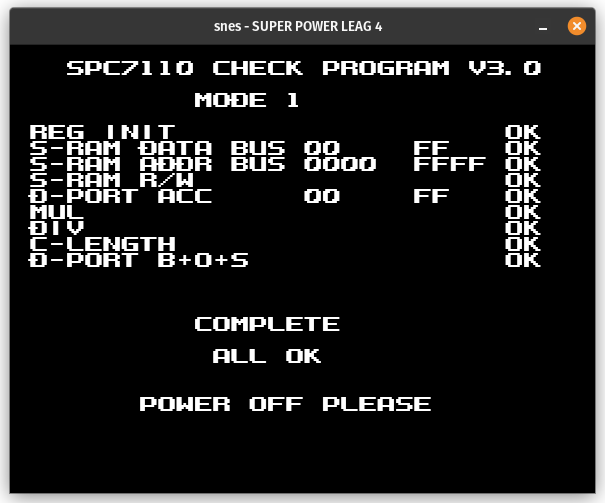
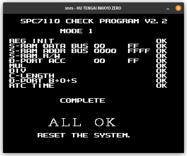
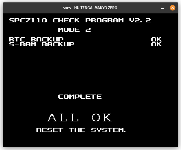
All three of the SPC7110 games include self-test functionality for the SPC7110 chip that runs automatically on boot if SRAM has not been initialized by the game. This test is not exhaustive, but it’s a good smoke test for whether basic SPC7110 functionality is working remotely correctly.
Tengai Makyou Zero’s self-test includes tests for its real-time clock chip so one of the other two games is better to start with. Here’s Super Power League 4:
One note for the self-test is that it expects reads from $4800 (next decompressed byte), $4810 (direct data ROM read #1), and $481A (direct data ROM read #2) to always return $00 before the respective feature has been initialized for the first time. The decompressor is initialized after the first write to $4806 (offset high byte), and direct data ROM reads are initialized after the first write to $4813 (highest byte of base address).
Another Clock
In addition to the rest of the SPC7110 chipset, Tengai Makyou Zero includes an Epson RTC-4513 real-time clock chip. I covered the basics of real-time clock chips in my half-post on the S-RTC chip so I won’t cover all of that again.
The RTC-4513 is more complex than the S-RTC, but thankfully there’s a publicly available datasheet that describes all the different registers and configurations (though Tengai Makyou Zero doesn’t seem to depend on all of them).
Time
RTC-4513 stores all time values in binary-coded decimal, same as the S-RTC chip. Notable differences are that month is stored as a separate ones digit + tens digit instead of using a single 4-bit value, and there is no century field - the chip can only store year values between 0 and 99. Software is responsible for interpreting what a specific year value means, e.g. as an offset from a start year.
To be precise, RTC-4513 times have the following fields:
- Seconds (0-59)
- Minutes (0-59)
- Hours (1-12 or 0-23 depending on configuration)
- AM/PM flag (only in 12-hour mode)
- Day (1-31)
- Month (1-12)
- Year (0-99)
- Day of week (0-6)
Unlike with S-RTC, Tengai Makyou Zero does use the day-of-week field, but the chip itself definitely doesn’t have any day-of-week logic - software is responsible for initializing the field.
Registers
The chip exposes 3 registers to the SNES CPU: a chip select line ($4840), a 4-bit data port ($4841), and a status register ($4842). In an emulator, the status register can return a constant $80 to indicate that the chip is always ready.
Internally, the chip has 16 registers that the SNES CPU can access through the data port:
- $0: Second, ones digit (0-9)
- $1: Second, tens digit (0-5)
- $2: Minute, ones digit (0-9)
- $3: Minute, tens digit (0-5)
- $4: Hour, ones digit (0-9)
- $5: Hour, tens digit (0-2) + AM/PM flag
- $6: Day, ones digit (0-9)
- $7: Day, tens digit (0-3)
- $8: Month, ones digit (0-9)
- $9: Month, tens digit (0-1)
- $A: Year, ones digit (0-9)
- $B: Year, tens digit (0-9)
- $C: Day of week (0-6)
- $D: Control register 1
- $E: Control register 2
- $F: Control register 3
There are also a few additional bits stuffed into some of the time field registers but Tengai Makyou Zero probably doesn’t depend on those. The most notable is the WRAP bit which indicates whether the time changed while the chip was selected. An emulator could avoid needing to emulate WRAP explicitly by latching the current time when the chip is selected through $4840.
The most notable flags in the control registers are the following:
- CAL/HW: Enables calendar functionality (day/month/year)
- 24/12: Configures 12-hour mode vs. 24-hour mode
- 30ADJ: Writing 1 to this bit rounds the current time to the nearest minute
- STOP/HOLD/RESET: Each of these stops the clock, with different side effects
The control registers also have some timer interrupt functionality but I don’t think Tengai Makyou Zero depends on it. The timer interrupt flag isn’t connected to the SNES CPU’s IRQ line, so the CPU would need to explicitly poll the interrupt flag from the RTC-4513 chip, and at that point it can already just read all of the time fields directly. I could be wrong though.
Reads/Writes
Reads work as following:
- Write 1 to $4840 (select chip)
- Write $C to $4841 ($C = read command)
- Write 4-bit register number to $4841
- Read 4-bit register value from $4841
- The register number automatically increments after each read, wrapping from $F to $0
- (Optional) Read additional 4-bit register values from $4841
- Write 0 to $4840 (deselect chip)
The CPU also reads $4842 at various points but that’s not important if the emulator is returning a constant value for the status register.
Writes work similarly:
- Write 1 to $4840 (select chip)
- Write $3 to $4841 ($3 = write command)
- Write 4-bit register number to $4841
- Write 4-bit register value to $4841
- Just like with reads, the register number automatically increments after the write
- (Optional) Write additional 4-bit register values to $4841
- Write 0 to $4840 (deselect chip)
The actual time-ticking can be implemented the exact same way as S-RTC, where the RTC state records the current system time at each update and advances based on the difference. Really, the additional complexity is all from dealing with the control register fields.
Finally
Tengai Makyou Zero has a self-test for the RTC chip:
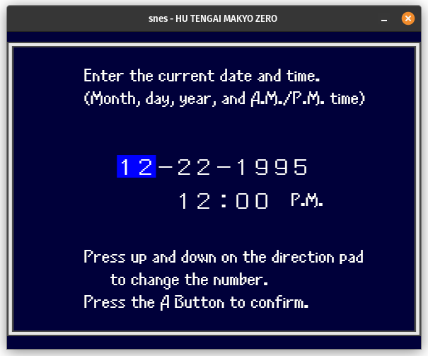
Once you get past the self-tests, it asks you set to the time, just as Daikaijuu Monogatari II does:
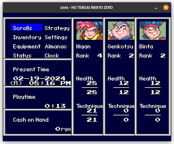
And then you can view the current time in the main menu:
Despite showing AM/PM, the game actually uses the RTC chip’s 24-hour mode - the AM/PM is purely a presentation thing in software.
The “Clock” sub-menu is only for making minor adjustments to the clock by rounding to the nearest minute, which uses the 30ADJ flag mentioned above.
What does the game actually use the RTC for? Well, according to this GameFAQs guide, a number of optional events occur only at specific times or days, and there are also optional events that require a certain amount of real time to pass (e.g. waiting for an egg to hatch). Some shops will also change their inventory at different times of day, and in one case there’s a ship route that changes its destination every few minutes. Still kind of gimmicky overall, but at least Tengai Makyou Zero uses it for more than Daikaijuu Monogatari II does.
One More
There’s only one SNES coprocessor that I haven’t covered, which happens to be the most well-known: the Super FX chip, which I’ll cover in the next (and last) post in this series.