The SA-1 coprocessor, or Super Accelerator 1, is a somewhat fascinating chip in that it has quite a lot of hardware that almost no games ever used. Its primary attraction is an additional 65816 CPU clocked at 3x the speed of the SNES CPU, and most of the SA-1 games only used it for that.
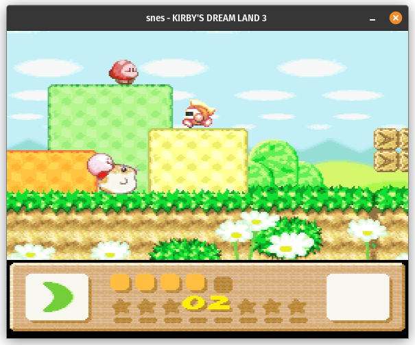
(Kirby’s Dream Land 3 hardly uses any of the SA-1 features, but it is a very pretty game)
Overview
SA-1 was the most widely used coprocessor. It was used in 35 games total, the most well-known being Super Mario RPG, Kirby Super Star, and Kirby’s Dream Land 3. Nearly all of the other SA-1 games are Japan-only, many of them shogi and go games, but there are a few that some might consider hidden gems like Marvelous: Mouhitotsu no Takarajima (aka Marvelous: Another Treasure Island) and Dragon Ball Z: Hyper Dimension.
The primary component in the SA-1 is an additional 65816 CPU (same model as the main SNES CPU) clocked at 10.74 MHz, three times as fast as the main CPU - and that’s before accounting for main CPU wait states from cartridge/WRAM accesses. It also has an on-chip multiplication/division unit that is significantly faster than the one in the SNES.
The main CPU can halt and reset the SA-1 CPU, and the two CPUs can signal interrupts to each other using SA-1 cartridge registers, but other than that the two CPUs operate completely independently. From here on out I’ll use “SNES CPU” to refer to the console’s 65816 CPU and “SA-1 CPU” to refer to the 65816 CPU on the cartridge board.
Ignoring the fact that it was much more expensive than a regular cartridge, the SA-1 was theoretically appealing to developers because they wouldn’t need to learn a new instruction set like they would have to do with something like the Super FX - the coprocessor CPU uses the exact same instruction set as the SNES CPU. The only complexity is in figuring out how to allocate work between the two CPUs and how to manage communication between them.
SA-1 cartridges have 2KB of I-RAM (instruction RAM) and a configurable amount of BW-RAM (backup/working RAM), usually between 8KB and 64KB. BW-RAM is generally battery-backed, but there is at least one game that has BW-RAM with no battery backup (Dragon Ball Z: Hyper Dimension). Both I-RAM and BW-RAM are fully accessible to both CPUs, and the cartridge has a bus collision detection circuit to gracefully handle both CPUs accessing cartridge ROM/RAM simultaneously.
The SA-1 has a number of other features that most SA-1 games don’t use:
- ROM banking through an MMC
- Runtime-configurable IRQ and NMI vectors for the SNES CPU
- A “bitmap view” of BW-RAM, accessible from the SA-1 CPU
- An H/V timer for the SA-1 CPU
- DMA between 2 of the 3 types of cartridge memory (ROM, I-RAM, BW-RAM)
- Variable-length bitstream reading
- Character conversion, hardware that converts bitmap graphics to the SNES bitplane format
Memory Map
The SNES CPU and the SA-1 CPU mostly share the same memory map, with a few differences. One of the most important differences is that the SA-1 CPU cannot access anything outside the cartridge. That means it can’t access WRAM, the PPU, the APU, or the SNES CPU’s on-chip registers (anything mapped to $4100-$43FF in the I/O area banks).
For ROM accesses, SA-1 cartridges have an MMC (memory management controller) that supports 4 mappable 1MB banks which can be read using either LoROM address mappings (A15 ignored) or HiROM address mappings (A15 not ignored).
For LoROM mappings:
- Banks $00-$1F, $8000-$FFFF: 1MB bank C
- Banks $20-$3F, $8000-$FFFF: 1MB bank D
- Banks $80-$9F, $8000-$FFFF: 1MB bank E
- Banks $A0-$BF, $8000-$FFFF: 1MB bank F
For HiROM mappings:
- Banks $C0-$CF, $0000-$FFFF: 1MB bank C
- Banks $D0-$DF, $0000-$FFFF: 1MB bank D
- Banks $E0-$EF, $0000-$FFFF: 1MB bank E
- Banks $F0-$FF, $0000-$FFFF: 1MB bank F
In practice, SA-1 games pretty much always leave bank C mapped to the first MB of ROM, bank D mapped to the second MB of ROM, bank E to the third MB of ROM, and bank F to the fourth MB of ROM. The MMC functionality is really only useful if a game has more than 4MB of ROM, and most (maybe all?) of the SA-1 games are 4MB or smaller, so the MMC feature was not really used.
The 2KB of I-RAM is mapped to $3000-$37FF in the I/O area banks. For the SA-1 CPU, it is additionally mapped to $0000-$07FF in the I/O area banks (which for the SNES CPU is mapped to the first 2KB of WRAM). I-RAM is small but it’s much faster than BW-RAM.
SA-1 cartridges theoretically support up to 256KB of BW-RAM but no game has that much - the most I’ve seen is 64KB. BW-RAM is mapped to 3 different locations, 2 for both CPUs and 1 for only the SA-1 CPU:
- The entirety of BW-RAM is mapped to banks $40-$4F
- $6000-$7FFF in the I/O area banks is a mappable 8KB BW-RAM bank; each CPU can map a different 8KB bank here
- (SA-1 CPU only) Banks $60-$6F provide a bitmap view of BW-RAM, which splits each byte into either 2-bit chunks or 4-bit chunks
Finally, the SA-1’s internal registers are all mapped to $2200-$23FF in the I/O area banks. $2200-$22FF are write-only registers and $2300-$23FF are read-only registers. Most registers are only accessible to one of the two CPUs, but almost all of the SA-1 DMA registers are accessible to both of them.
Arithmetic
The SA-1 CPU has access to a multiplication/division unit that is much, much faster than the one in the SNES while also supporting larger numbers. It can perform 3 different operations:
- Multiplication: signed 16-bit x signed 16-bit = signed 32-bit
- Division: signed 16-bit / unsigned 16-bit = signed 16-bit quotient, unsigned 16-bit remainder
- Multiply-accumulate: signed 16-bit x signed 16-bit multiplication accumulated into a signed 40-bit sum
Multiplication and division take 5 SA-1 CPU cycles while multiply-accumulate takes 6 SA-1 CPU cycles. Like with the SNES multiplication/division unit, the SA-1 CPU can do other things while waiting for a multiply/divide operation to finish, but games will often just use a few nop instructions to wait until the arithmetic operation is done.
For comparison, this is what the SNES CPU can do:
- Multiplication: unsigned 8-bit x unsigned 8-bit = unsigned 16-bit
- Division: unsigned 16-bit / unsigned 8-bit = unsigned 16-bit quotient, unsigned 16-bit remainder
Multiplication takes 8 SNES CPU cycles (at least 24 SA-1 CPU cycles), and division takes 16 SNES CPU cycles (at least 48 SA-1 CPU cycles). That is significantly slower on top of working with smaller / less precise numbers!
The SNES CPU does have access to a signed multiplication unit in the PPU that can perform signed 16-bit x 8-bit = 24-bit multiplication very quickly, so quickly that it’s guaranteed to be done by the time the CPU can start reading the result, but this multiplication unit is inaccessible while the PPU is in Mode 7 and actively rendering (because the PPU is using it).
Inter-CPU Communications
Since the SA-1 CPU can’t drive the PPU or the APU, some amount of coordination between the two CPUs is necessary to get anything useful out of the SA-1 CPU.
Some games might treat the SA-1 CPU as a task executor, where the SNES CPU delegates specific expensive computations to it and then waits for it to finish. Other games might delegate most game logic to the SA-1 CPU while only using the SNES CPU for DMA and PPU/APU access. Yet other games might find ways to parallelize tasks so that both CPUs can do useful work in parallel.
There are a few ways that the two CPUs can talk to each other:
- Shared cartridge RAM (I-RAM and BW-RAM)
- Software interrupts
- The SA-1 CPU can generate IRQ for the SNES CPU, and the SNES CPU can generate both IRQ and NMI for the SA-1 CPU
- A 4-bit “message” in each of the CPU control registers
- The SNES CPU can halt or reset the SA-1 CPU
Unlike with other coprocessors, the SNES CPU can safely access cartridge memory while the SA-1 CPU is actively using it. The cartridge has a bus collision detection circuit that will stall the SA-1 CPU if necessary in order to avoid bus conflicts. However it’s not ideal to have both CPUs frequently accessing the same type of cartridge memory as that will effectively slow down the SA-1 CPU.
Beyond shared memory, communication occurs mainly through control registers on the SA-1 chip. The SNES CPU has access to registers that allow it to do the following:
- Halt the SA-1 CPU
- The SA-1 CPU is halted at power-on so that it doesn’t behave unpredictably due to uninitialized RAM and registers
- Reset the SA-1 CPU
- This is useful to guarantee that the SA-1 CPU begins execution from a known state
- Set the SA-1 CPU’s IRQ, NMI, and RESET vectors
- When the SA-1 CPU reads from one of these interrupt vector addresses, the SA-1 chip will return the configured vector instead of reading from ROM
- Generate IRQ or NMI for the SA-1 CPU
- Acknowledge IRQs generated by the SA-1 CPU
- Send a 4-bit “message” that the SA-1 CPU can read through a register
- Read a 4-bit “message” sent by the SA-1 CPU through a register
The SA-1 CPU has access to registers that allow it to do the following:
- Generate IRQ for the SNES CPU
- Acknowledge IRQs and NMIs generated by the SNES CPU
- Send/read 4-bit “messages” to/from the SNES CPU through a register
- Specify that the SNES CPU should read its IRQ and NMI vectors from SA-1 I/O registers instead of ROM
- Almost no games use this feature
Timings
The SA-1 CPU runs at 10.74 MHz (SNES mclk/2), but much like the SNES CPU, certain types of memory accesses will cause wait states and effectively slow down the SA-1 CPU. I-RAM accesses incur no wait states (unless there’s a bus collision), ROM accesses sometimes do, and BW-RAM accesses always do.
Before going into more detail, I’ll note that from an emulation perspective it’s not really necessary to emulate these precise timings unless you’re going for very high accuracy. Games seem to be not very sensitive to the SA-1 CPU running a bit too fast compared to actual hardware.
I-RAM supports 8-bit memory accesses at the full 10.74 MHz speed. The SA-1 CPU will only get a wait state accessing I-RAM if the SNES CPU accesses I-RAM during the same 10.74 MHz cycle, in which case the SA-1 CPU stalls for a single 10.74 MHz cycle due to the bus collision detector (which always gives priority to the SNES CPU).
BW-RAM supports 8-bit memory accesses at half speed, or 5.37 MHz. The SA-1 CPU is stalled for a single 10.74 MHz cycle every time it accesses BW-RAM. Bus collisions with the SNES CPU cause the SA-1 CPU to stall for a full 5.37 MHz cycle, or equivalently two 10.74 MHz cycles. Because of this games should generally use I-RAM for coordination between the two CPUs rather than BW-RAM.
ROM also supports memory accesses at only 5.37 MHz, but the SA-1 CPU has a 16-bit data bus to ROM which allows it to avoid wait states in many cases by loading 2 bytes per 5.37 MHz cycle. The main exceptions seem to be jump/branch/return instructions, which either always or sometimes incur a wait state as the CPU changes the ROM address that it’s reading from. I would guess that memory reads for 16-bit values at odd addresses also likely cause a wait state.
Bus collisions with the SNES CPU are more severe in ROM because the SA-1 CPU must wait for a full 5.37 MHz cycle if it collides with a ROM access from the SNES CPU, when normally the SA-1 CPU gets few/no wait states when reading from ROM (unlike BW-RAM). Ideally the SNES CPU will operate primarily out of WRAM while the SA-1 CPU is making lots of ROM accesses.
DMA from ROM to I-RAM copies 1 byte per 10.74 MHz cycle. Other types of DMA (ROM to BW-RAM, I-RAM to BW-RAM, BW-RAM to I-RAM) copy 1 byte per 5.37 MHz cycle. (Although very few games use SA-1 DMA at all.)
Lesser-Used Features
Now for features that very few SA-1 games used.
DMA
The simplest little-used feature is SA-1 DMA, which supports copying data between different types of cartridge memory. The only real bit of complexity here is that the SA-1 CPU may or may not be stalled during DMA.
DMAs that read from ROM will always stall the SA-1 CPU until the DMA finishes. For DMAs that copy between I-RAM and BW-RAM, there is a control bit that the SA-1 CPU can set that configures whether or not the CPU stalls during DMA. If it’s not stalled, it’s unclear exactly what happens if the SA-1 CPU accesses I-RAM or BW-RAM while a DMA is in-progress.
Presumably SNES CPU accesses during SA-1 DMA are gracefully handled by the bus collision detector.
DMA is used by at least 3 games: Marvelous, J.League ‘96, and Jumpin’ Derby (you’ll see this name again). Marvelous also gets a mention for being one of the few SNES games that enables color math while in the high-resolution Mode 5.
Timer
The SA-1 has a timer for the SA-1 CPU that mimics the SNES CPU’s H/V timer. It works pretty much the same way, except it can be configured to either HV mode (function same as SNES timer) or linear mode (both H and V count from 0 to 511). Similar to the SNES timer, it can generate H/V/HV IRQs for the SA-1 CPU when the timer crosses specific values, but I don’t believe any games used this functionality.
BW-RAM Bitmap View
The SA-1 CPU has access to a read/write bitmap view of BW-RAM that splits each byte into either 2-bit chunks or 4-bit chunks, with each chunk accessible at a different address. This is theoretically useful for reading/writing 2bpp or 4bpp bitmap pixel data because it removes the need for the CPU to shift and mask to access different pixels - it can just access different addresses.
In 2bpp bitmap view mode, bitmap view addresses are mapped to physical BW-RAM as following:
|
|
4bpp works the same way except the shifts and masks are different.
Variable-Length Bitstream Reading
SA-1 has a variable-length bitstream feature where you can point it at an address in ROM and it will expose the data at that address in the form of a 16-bit shift register that automatically fills itself with more bits from ROM as needed. This is useful for reading blocks of compressed data where each compressed chunk could be a different number of bits, and you don’t know ahead of time how many bits each chunk of data will be (e.g. because the size depends on previous data in the bitstream).
Only one game used this feature, Jumpin’ Derby.
To be more concrete, an emulated implementation might look something like this:
|
|
One thing I didn’t handle there is that the VDA register contains an SA-1 bus address, not exactly a ROM address, so an emulator needs to map the address before reading from ROM. Jumpin’ Derby specifically does variable-length bitstream reads from addresses in the $D00000-$DFFFFF range, which should map to the second MB of its 2MB ROM (with HiROM address mapping).
Documentation says that this feature has an auto-increment mode, but it’s unclear how it works and not one game uses it. Some documentation suggests that auto-increment doesn’t work at all.
Character Conversion
Easily the most complex of the little-used SA-1 features, character conversion is meant to convert bitmap graphics to the SNES bitplane graphics format, and it’s capable of doing so on-the-fly while the SNES is reading via DMA. In theory this allows the SA-1 CPU to draw graphics in a bitmap format and then have the hardware automatically convert those graphics to the proper SNES format while SNES DMA copies the converted graphics directly into PPU VRAM.
There are two types of character conversion DMA: automatic (“type 1”) and semi-automatic (“type 2”). Both types can be configured to convert 2bpp tiles, 4bpp tiles, or 8bpp tiles, and both types operate using a buffer in I-RAM that stores 2 rows of 8 pixels each. At any given time, SNES DMA is reading out one of the two 8-pixel rows in the I-RAM buffer while CCDMA is writing the next row of pixels to the other half of the buffer.
Type 1 CCDMA (automatic) reads its source data out of BW-RAM. It treats BW-RAM as what documentation calls “virtual VRAM”, where BW-RAM is interpreted as if it’s a 2D grid of 8x8 bitmap tiles with a configurable width. The width matters because data is transferred tile-by-tile rather than simply pixel-by-pixel, and the CCDMA unit needs to know how many tiles are in a row in order to calculate the correct BW-RAM address for each row of pixels in each tile.
Once automatic CCDMA starts, the SNES CPU waits for a character conversion IRQ to signal that the first tile is ready to copy, then it starts a DMA reading from BW-RAM. The SA-1 cartridge automagically notices when the DMA starts, and instead of returning bytes directly from BW-RAM it returns output from the CCDMA unit (stored in the I-RAM buffer) which is converting graphics tile-by-tile. The SA-1 hardware syncs itself to SNES DMA timing to guarantee that it won’t get too far ahead of DMA reads. The CCDMA unit will continue doing this forever until the SA-1 CPU manually stops it, which it will do after the SNES DMA completes.
Type 2 CCDMA (semi-automatic) is, as the name implies, more manual. The SA-1 CPU manually writes a row of 8 bitmap pixels to a set of registers, and once the 8th pixel is written the CCDMA hardware will automatically convert it to the SNES bitplane format and write the output to one half of the I-RAM buffer. The SNES CPU then initiates a short DMA to copy that row of pixels from I-RAM to PPU VRAM while the SA-1 CPU starts writing the next row of pixels. Software is responsible for ensuring that the SA-1 CPU doesn’t get ahead of the SNES CPU (or vice versa).
This feature was only used by 3 games, SD Gundam G NEXT (a Japan-only Gundam strategy game) and 2 Japan-only golf games. Here are 2 screenshots of Pebble Beach no Hatou New (one of those golf games), which uses character conversion DMA to render the background:
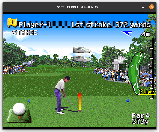
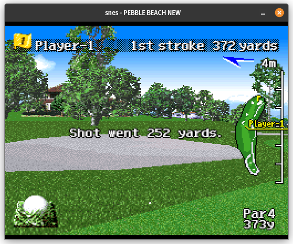
This is actually quite impressive for the SNES, but unfortunately the game pauses for several seconds every time it needs to redraw the background.
Why Does This Chip Exist?
The SA-1 is peculiar among the coprocessors because of how much hardware it has that almost no games used, including Nintendo’s own SA-1 games. It also came very late in the SNES lifespan, with the first SA-1 games releasing in 1995 - only one year before the Nintendo 64 launched. So why did Nintendo create SA-1?
One theory I’ve seen is that the SA-1 was built out of hardware that was repurposed from the canceled SNES CD add-on, and having worked on a Sega CD emulator, I can believe it.
The Sega CD also added an additional CPU of the same model as the console’s CPU (a 68000 in this case) but clocked faster. It has a 256KB block of RAM called “word RAM” that is shared between the two CPUs, though they can’t access it simultaneously. Typically the Sega CD CPU reads and processes data from the CD-ROM into word RAM, and then the Genesis CPU initiates a DMA from word RAM into VRAM (or does whatever else it needs to with the processed data). SA-1’s BW-RAM serves the same function as Sega CD’s word RAM, although SA-1 obviously doesn’t have a CD-ROM drive attached.
SA-1’s character conversion hardware in particular seems like it would have been useful for playing FMV movies. The video frames could be stored on CD-ROM in a compressed bitmap format, the SA-1 CPU could decompress the bitmap data into BW-RAM (possibly using the variable-length bitstream feature to read the compressed data), and then the character conversion hardware could convert the decompressed bitmap graphics to SNES bitplane graphics that the SNES CPU could DMA directly into VRAM. Something like this was less necessary with Sega CD because the Genesis VDP uses a packed pixel format rather than a bitplane format, but it does have hardware to create a word RAM view that automatically splits bytes into 4-bit pixels at different addresses - very similar to SA-1’s BW-RAM bitmap view.
Of course, the Sega CD also had a decent amount of other hardware in it (probably why it was so expensive), but that’s a separate topic.
MSU-1
An alternative view of what the SNES CD might have looked like is the MSU-1 (Media Streaming Unit 1), a virtual coprocessor created by Near (the author of bsnes). MSU-1 never existed in actual SNES cartridges, but it was designed such that it could be implemented as a cartridge coprocessor that will work with an unmodified SNES console. In fact, some flash cartridges support MSU-1 games on actual hardware.
MSU-1 is significantly simpler than SA-1. It supports up to 4GB of additional storage in addition to cartridge ROM (yes that’s 4 gigabytes), it has some registers that allow the SNES CPU to access the additional storage through a seek-and-read API, and it supports audio playback of uncompressed 16-bit PCM samples at 44.1 KHz (very similar to CD audio although the format is slightly different). Unlike SA-1 it doesn’t put any processing hardware inside the cartridge, unless you count the audio playback as processing hardware. This is actually somewhat similar to the CD-ROM add-on for the PC Engine / TurboGrafx-16 which is pretty much just a CD-ROM drive, CD audio support, and lots of additional RAM (which the PCE desperately needed).