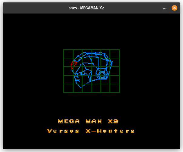
The Cx4, or Capcom Consumer Custom Chip, is a coprocessor that Capcom used in Mega Man X2 and Mega Man X3. It’s most well-known as the coprocessor that enables those games’ 3D wireframe models, but they also use it for sprite scaling/rotation effects and to help out with managing the sprite table.
Some History
The Cx4 is particularly interesting among the coprocessors that contain CPUs/DSPs in that for a long time, no one knew much of anything about the processor inside of it. It was identified through decapping as a Hitachi HG51B169 DSP driven by a 20 MHz clock, but there was virtually no public information on this DSP which made emulating it at a low level completely impossible. Similar to DSP-1, early SNES emulators were forced to HLE the Cx4 chip to get Mega Man X2 & X3 working.
Even the HLE implementations involved quite a bit of reverse engineering, though of the game code rather than the processor itself. The game interacts with the chip by writing values to a bunch of on-chip registers and sometimes on-chip RAM, and then writing what appears to be a command. After that, the game spin loops while polling a Cx4 status register to wait for it to finish execution. Creating an HLE implementation required reverse engineering every single command based solely on what the game code did before and after each command.
A lot of the results of that reverse engineering work are documented in Anomie’s C4 document (early documentation tends to refer to this chip as C4 rather than Cx4). This document gives significant insight into what the games use the chip for, and fortunately there are very few differences between MMX2 and MMX3 in this regard. Here is the list of commands from Anomie’s doc:
 00: Sprite functions
 01: Draw wireframe
 05: Propulsion (?)
 0d: Set vector length
 10: Convert polar coordinates to rectangular
 13: Convert polar coordinates to rectangular
 15: Pythagorean
 1f: atan
 22: Trapaziod
 25: Multiply
 2d: Transform Coords
 40: Sum (test)
 54: Square (test)
 5c: Immediate Reg (test)
 89: Immediate ROM (test)
And this is how “sprite functions” are refined:
  When $00 is written to $7f4f, the subfunction specified in $7f4d is
  performed.

  00: Build OAM
  03: Scale/Rotate
  05: Transform Lines
  07: Scale/Rotate
  08: Draw wireframe
  0b: Disintergrate
  0c: Wave
Each command is described in terms of its inputs and outputs, and how exactly to generate the outputs from the inputs for HLE purposes. As an example, here’s the description for one of the simplest commands:
25: Multiply
------------

  Input:
    $7f80-2: Multiplicand A
    $7f83-5: Multiplicand B

  Output:
    $7f80-2 or $7f80-5: Product

  This seems to multiply the 3-byte word in $7f80 with the 3-byte word in
  $7f83, and write the result back to $7f80. That's all. MMX2 uses it at that
  infamous point in the Overdrive Ostrich stage.
The wireframe command’s description is light on details regarding the math required, but other than that you could feasibly write a new HLE implementation using only this document - it’s quite thorough.
Low-Level Emulation
The primary goal of bsnes during development was to emulate the SNES as accurately as possible, in contrast to earlier emulators like ZSNES and early versions of Snes9x that focused on just getting the popular games working decently. This goal included emulating every SNES coprocessor at a low level, including the less well-understood DSPs like DSP-1 and Cx4. A 2012 article from the author of bsnes describes what was required to LLE the quirkier DSPs, including Cx4.
The first important discovery was someone realizing that the Cx4 DSP doesn’t have an on-chip program ROM like DSP-1 does. Instead, the Cx4 program is stored directly in cartridge ROM, like with the Super FX. Interestingly, the Cx4 program is nearly byte-for-byte identical between Mega Man X2 and X3 - the only difference is a byte that’s used to determine where the wireframe model data is stored in ROM.
Once the Cx4 program was located in cartridge ROM, someone was somehow able to reverse engineer the DSP’s entire instruction set (or at least the subset that MMX2/MMX3 use) by cross-referencing the raw program bytes for each command/function with the existing emulator HLE implementations. I personally find that extremely impressive given that there was previously zero public documentation on this ISA!
With the ISA reverse engineered, someone else found an exploit in the MMX2/MMX3 code that made it possible to dump the Cx4’s on-chip data ROM, the final piece necessary to make LLE possible. The data ROM only contains math lookup tables so it would have been possible to recreate it, but even in that scenario the dump is very important for verifying that a recreation is a bit-for-bit match with the actual cartridge’s data ROM.
And thus, bsnes became the first emulator with a functional LLE implementation for the Cx4.
Specifications
As mentioned earlier, the Cx4’s primary component is a Hitachi HG51B169 DSP clocked at 20 MHz, although instruction timings and possible wait states are unknown. Opcodes are 16-bit while registers and ALU operations are 24-bit. It has 16 general-purpose 24-bit registers. It can perform signed 24-bit x 24-bit multiplication in a single instruction, although it’s supposedly necessary to insert a one-instruction delay after executing one of the multiplication instructions.
The Cx4 chip also has 3KB of on-chip RAM that is accessible by both the DSP and the SNES CPU (though not simultaneously), as well as a 3KB data ROM (1,024 x 24-bit words). The data ROM contains lookup tables for 6 different math functions: Division, square root, sine, cosine, tangent, and arcsine. That’s all that’s in there, and it’s possible to recreate it bit-for-bit as long as you know where each lookup table is located, how large it is, what the range of input values is, and what the scale is.
The DSP remains idle until the SNES CPU starts it up by writing to its instruction pointer register, after which it begins execution at wherever the SNES CPU told it to. The SNES CPU makes the DSP execute different “commands” by having it start execution at different addresses. Once started, the DSP continues executing instructions until it executes a special stop opcode which causes it to halt until the SNES CPU spins it up again. It exposes a status register that the SNES CPU can read to see whether the DSP is running or halted.
One quirk with the Cx4 is that, similar to Super FX, the SNES CPU can’t access cartridge ROM or Cx4 RAM while the DSP is actively running. It can configure NMI and IRQ vectors through Cx4 registers in case an interrupt triggers while the DSP is running, and the Cx4 will return the configured vectors if the CPU accesses the interrupt vector addresses while the DSP is active.
Memory Map
Mega Man X2 and Mega Man X3 both use a standard LoROM mapping for ROM addresses, and neither game has SRAM.
Cx4’s 3KB RAM is mapped to $6000-$6BFF in the I/O area banks ($00-$3F + $80-$BF).
All of the Cx4 registers are mapped to $7F40-$7FAF in the I/O area banks. Other than the status register at $7F5E, most of these are probably not accessible by the SNES CPU while the DSP is running.
These are all of the registers exposed to the SNES CPU:
- $7F40-$7F42: Cx4 DMA source address in ROM
- $7F43-$7F44: Cx4 DMA length
- $7F45-$7F46: Cx4 DMA destination address in Cx4 RAM
- $7F47: Initiate Cx4 DMA
- $7F49-$7F4B: DSP program ROM base address (in cartridge ROM)
- $7F4D-$7F4E: DSP instruction page
- $7F4F: DSP instruction pointer
- Writing to this address causes the DSP to start execution at the given instruction page+pointer within program ROM
- $7F5E: DSP status register (used only to know whether the DSP is actively running)
- $7F6A-$7F6B: NMI vector (when DSP is running)
- $7F6E-$7F6F: IRQ vector (when DSP is running)
- $7F80-$7FAF: DSP’s 16 general-purpose 24-bit registers
- These are exposed to the SNES CPU because they’re often used for function inputs and/or outputs
Other addresses in the $7F40-$7FAF range are either registers with unknown functionality or unmapped addresses.
Cx4 DMA is a simple ROM-to-RAM copy that is presumably faster than manually copying data using either the SNES CPU or the DSP. SNES DMA can’t be used to copy from ROM to Cx4 RAM because it can only copy between address bus A (cartridge + WRAM + CPU registers) and address bus B (PPU ports + APU ports + WRAM ports). It can’t do a cartridge-to-cartridge copy.
Instruction Set
This seems like a good time to mention that Mega Man X2 and X3 both have built-in self-test functionality for the Cx4 chip that you can execute by holding B on controller 2 while the game boots:
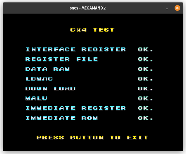
This test is written to exercise specific DSP opcodes and data ROM validity rather than exhaustively testing every single DSP routine, so it’s not super helpful for validating an HLE implementation, but it is really helpful for (mostly) validating an LLE implementation.
The best resources I’ve seen for low-level Cx4 documentation are nocash’s fullsnes documentation and Overload’s site. The latter went offline in 2023 because it was hosted through an ISP and the ISP shut down their user site hosting, but thankfully it’s archived.
All instructions are represented using a single 16-bit opcode. The highest 6 bits define the operation and the lowest 10 bits often contain operation parameters.
Many instructions take an 8-bit register number as an operand (embedded in the opcode), but that register is not necessarily an actual DSP register. It can be any of the following:
- The 24-bit accumulator
- Either half of the most recent 48-bit multiplication result
- One of the 16 general-purpose registers
- Buffers for reading from cartridge ROM, Cx4 data ROM, or Cx4 RAM
- The DSP can’t read directly from ROM/RAM during ALU operations - it has dedicated instructions that read from ROM/RAM into a buffer, and then it can use the buffers as ALU operands
- The current cartridge ROM pointer, data ROM pointer, or Cx4 RAM pointer
- One of 16 “immediate registers” that always return a specific constant value
ALU
The DSP supports the following ALU operations:
- Add, subtract, and reverse subtract (reverse being
operand - Ainstead ofA - operand) - Compare and reverse compare
- Bitwise AND, OR, and XOR
- Left shift, arithmetic right shift, logical right shift, and rotate right
- All of these use the operand as the shift/rotate count
- Sign extend the lowest 8 or 16 bits of the accumulator
- Signed multiplication, 24-bit x 24-bit = 48-bit
- This is supposedly slower than the other ALU instructions, making it necessary to execute at least one additional instruction (usually a no-op) before reading the multiplication result
All instructions except sign extension can take either an 8-bit register number operand or an 8-bit immediate operand, both embedded in the lowest 8 bits of the opcode.
All instructions except for multiplication and sign extension support applying a left shift to the accumulator before the ALU operation. The shift count is embedded in the opcode and can be set to 0, 1, 8, or 16.
Loads
The DSP supports the following basic load operations:
- Move into accumulator from register number operand / 8-bit immediate operand
- Move into register number operand from accumulator
- Move into instruction page buffer from register number operand / 8-bit immediate operand
- These instructions do not immediately modify the instruction page; the DSP must execute a far jump instruction to copy the page buffer into the instruction page
- There is also a variant of this instruction that only updates 1 of the 2 bytes instead of updating all 15 bits
- Swap the accumulator with a register number operand
It also supports the following operations for interacting with ROM/RAM:
- Read a value into the cartridge ROM buffer using the current cartridge ROM pointer
- Increment the cartridge ROM pointer
- Read a value into the data ROM buffer using the current data ROM pointer
- Read a value into the Cx4 RAM buffer, with RAM address specified by either a register number operand or the current Cx4 RAM pointer with an 8-bit immediate index
- Write a value into Cx4 RAM from the Cx4 RAM buffer, with RAM address specified the same way as with reads
Data ROM reads are 24-bit operations while cartridge ROM reads and Cx4 RAM reads/writes are 8-bit operations. However, the RAM buffer is 24-bit - the opcodes for accessing RAM use 2 of the opcode bits to specify which of the 3 bytes should be read into / written from.
It is supposedly necessary to execute a special “finish” opcode after every cartridge ROM read, but it’s unclear what this actually does.
Jumps
The DSP supports the typical jump instructions: conditional and unconditional jumps, conditional and unconditional calls, and unconditional return. It has a hardware call stack with a size of 8 (probably, I’ve seen some documentation that says it’s 16). Jumps and calls update the instruction pointer using an 8-bit immediate value embedded in the opcode.
The DSP also supports a conditional “skip” instruction that skips over the next opcode if the condition is true.
The only thing that’s really notable about jumps is that jumps and calls can be either near or far, specified using a single bit in the opcode. A near jump only updates the 8-bit instruction pointer, while a far jump updates both the 8-bit instruction pointer and the 15-bit instruction page. The instruction page is set based on the current contents of the DSP’s instruction page buffer.
Returns always update both the instruction pointer and the instruction page, pulled from the call stack.
Timings
All Cx4 timings are completely unknown as far as I know, beyond the fact that the DSP is driven by a 20 MHz oscillator on the cartridge board. If you wanted to try and emulate Cx4 timing, you could assume that every instruction takes one 20 MHz cycle, and that is guaranteed to run at least as fast as actual hardware.
Mega Man X2 and Mega Man X3 are not sensitive to the DSP running too fast - in fact, they’ll work fine if the DSP finishes every routine instantly from the game’s perspective, which is what I do in my emulator. When the SNES CPU writes to the DSP’s instruction pointer register, I have the DSP continuously execute instructions until it executes a stop opcode (most significant 6 bits are all 1s).
Conclusion
While many of its inner workings are still unknown, it’s clear that the Cx4 chip was quite a powerful processor for its time. It’s comparable to the Super FX in raw computational power, although it doesn’t have anything like the Super FX’s custom graphics plotting hardware. Makes you wonder what it would have been capable of if Capcom had used it in more than 2 games.