While Sega tried to expand the Genesis’ capabilities by adding on to the console hardware with the Sega CD and 32X, Nintendo took a different approach with the SNES: put additional hardware into the cartridge on a game-by-game basis. This post will cover the first SNES coprocessor, DSP-1, and its close relatives.
DSP-1
The very first game to use a coprocessor was Pilotwings, released in Japan in late 1990. It contains a coprocessor called DSP-1 which is an NEC μPD77C25 DSP pre-programmed with math routines to assist in 3D calculations.
DSP-1 was used by around 16 games, most notably Pilotwings and Super Mario Kart.
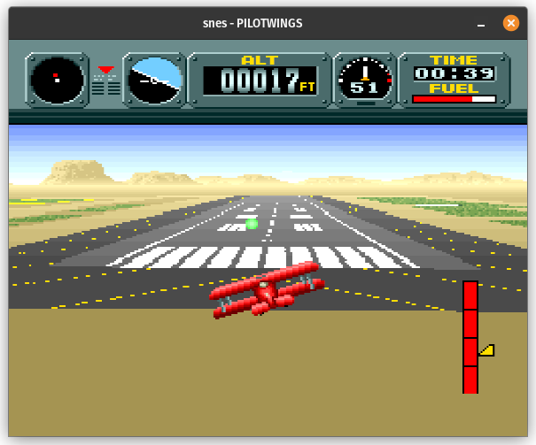
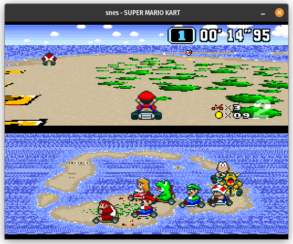
Pilotwings and Super Mario Kart both use the SNES PPU’s Mode 7 to render their faux-3D graphics with perspective, but they rely very heavily on the DSP-1 to perform the 3D calculations required for each frame. Without the coprocessor they would have a really hard time maintaining 60 frames per second.
The DSP
The DSP itself is clocked at 8 MHz and can execute one instruction per cycle. Opcodes are 24-bit, and each opcode is one of three basic operations: load, jump, or ALU (arithmetic logic unit). Importantly, the DSP can perform signed 16-bit x 16-bit multiplication in a single cycle which is extremely helpful for doing 3D calculations. It doesn’t support floating-point operations, but ALU operations can use either half of the 32-bit multiplication result as an operand, so programs will often operate in fixed-point decimal with a 16-bit integer part and a 16-bit fractional part.
The chip supports 6KB of program ROM (2048 x 24-bit opcodes), a 2KB data ROM (1024 x 16-bit words), and 512 bytes of on-chip data RAM (256 x 16-bit words). DSP-1 fills the data ROM with math lookup tables (e.g. sine tables), and the program ROM is a simple routine that can execute various math functions in response to commands from the SNES CPU.
Load and jump do pretty much what you would expect, but the ALU operation is interesting because it can do lots of things at once:
- Read input operand from a register, data ROM, data RAM, or one half of the current multiplication result
- Perform 1 of 15 ALU functions (or a no-op) using 1 of 2 accumulator registers
- The 15 count does not include multiplication; multiplication is automatic based on the current contents of the K and L registers
- Perform a load operation in addition to the ALU function
- Automatically adjust the data RAM pointer after the operation
- Automatically decrement the data ROM pointer after the operation
- Perform a return by popping from the call stack
Needing to fit all of those parameters is why opcodes are 24-bit. ALU opcodes use:
- 1 bit to identify ALU vs. load/jump
- 4 bits for ALU function (no-op if set to 0)
- 4 bits for source register
- 4 bits for destination register (for the load; no load is performed if set to 0)
- 2 bits for ALU input operand
- Source register, data RAM, or multiplication result low/high byte
- 1 bit for which accumulator to use with the ALU function
- 2 bits for how to adjust the lowest 4 bits of the data RAM pointer
- No-op, increment, decrement, or set to zero
- 4 bits for how to adjust the highest 4 bits of the data RAM pointer
- These bits are XORed with the highest 4 bits of the data RAM pointer after the operation
- 1 bit for whether to auto-decrement the data ROM pointer
- 1 bit for whether to pop from the call stack and return
That’s all 24 bits!
The actual ALU functions are mostly what you would expect:
- Bitwise OR, AND, XOR, and NOT
- Add and subtract, with and without carry
- Increment and decrement
- Arithmetic right shift by 1
- Rotate bits left by 1, through carry flag
- Shift bits left by 2 or 4
- Weirdly, this operation fills the low bits with 1s instead of 0s
- Swap bytes
SNES Integration
The SNES CPU communicates with the coprocessor using only two 8-bit registers: a data register and a status register. LoROM / mode $20 cartridges map these registers to $8000-$FFFF in banks $30-$3F / $C0-$CF, while HiROM / mode $30 cartridges map these registers to $6000-$7FFF in banks $00-$0F / $80-$8F.
The DSP’s data register is internally 16-bit, but it can be configured to function as either an 8-bit register or a 16-bit register. When it’s in 16-bit mode, reads/writes from the SNES CPU alternate between accessing the low byte and the high byte.
The status register contains a few flags indicating current DSP status, most importantly the RQM flag (request for master) which indicates whether the DSP is waiting for a read/write from the SNES CPU. The RQM flag is automatically cleared every time the SNES CPU fully accesses the data register: after every access in 8-bit mode, and after every high byte access in 16-bit mode.
The DSP-1 program is fairly simple in structure. It begins by setting the data register to 8-bit mode and then looping until the SNES CPU writes a command byte to the data register. It then sets the data register to 16-bit mode and calls a function based on the command sent. Each function reads its input parameters through the data register, performs some calculations, and then writes the outputs back out through the data register before returning back to the beginning of the program to wait for the next command.
The only command that doesn’t quite follow this structure is command $0A, the “raster” command, which calculates how the background layer should be scaled/rotated on each scanline based on a configured 3D projection. It outputs an infinite series of line-by-line Mode 7 matrix parameters (A/B/C/D), only stopping when the SNES CPU tells it to stop by writing a specific value to the data register instead of reading the next parameter from it. This command is designed to be used with HDMA, where the HDMA channel will copy the four Mode 7 parameters from the data register to the PPU before each scanline. This allows the DSP to do perspective calculations while minimizing the amount of work that the SNES CPU needs to do.
Emulation
Most SNES emulators emulate the DSP-1 using what’s called an HLE implementation, or high-level emulation. Instead of directly emulating the DSP chip, they emulate the functionality that the DSP-1 program provides: whenever the SNES CPU sends a command, wait for it to send the inputs through the data register, then emulate that command’s functionality using a simple function call and make the outputs available through the data register.
Early emulators had to use HLE implementations because the DSP hadn’t been reverse engineered yet and because the DSP-1 program ROM hadn’t been dumped. Modern emulators often still use an HLE implementation, partly because it’s more efficient but mainly because the DSP-1 program ROM is copyrighted code and can’t be legally distributed with an emulator.
bsnes, ares, and other high-accuracy emulators additionally contain LLE implementations, or low-level emulation. An LLE DSP-1 implementation does directly emulate the μPD77C25 DSP, which is less performant but more accurate. However LLE implementations do require the user to supply a DSP-1 program ROM in order to function. (The data ROM is less of an issue as it’s just math lookup tables.)
My own emulator uses an LLE implementation because I couldn’t find thorough enough documentation on the DSP-1 program to make it possible to HLE without either reverse engineering the program myself or copying code from another emulator, neither of which I wanted to do. It’s not enough to know the math behind each command - you have to precisely emulate exactly how the DSP-1 implements those math functions in terms of scale, precision, order of operations, etc.
One final interesting tidbit is that there are 3 different variants of the DSP-1: the original DSP-1, DSP-1A, and DSP-1B. Original DSP-1 and DSP-1A seem to be identical other than minor hardware differences, while DSP-1B modifies the program ROM to fix a bug in one of the math functions. Pilotwings accidentally depends on this bug for its plane attract demo to work correctly, and if it’s run with the DSP-1B program ROM, the plane will crash instead of landing successfully:
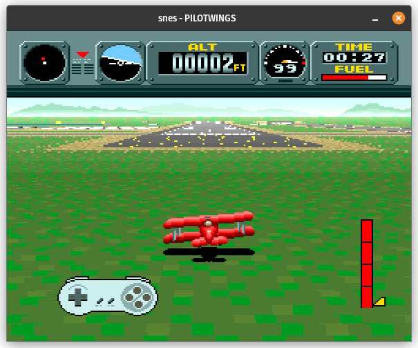
Interestingly, actual Pilotwings cartridges were manufactured both with and without DSP-1B, so this bug can occur even on actual hardware depending on which chip is in the particular cartridge.
DSP-2 / DSP-3 / DSP-4
There were 3 other coprocessor chips that used the μPD77C25 DSP: DSP-2, DSP-3, and DSP-4. The only difference between these three (and DSP-1) is that each chip uses different program and data ROMs.
Each of these was used only by a single game: Dungeon Master (DSP-2), SD Gundam GX (DSP-3), and Top Gear 3000 (DSP-4).
DSP-2 is designed pretty much specifically for Dungeon Master. The game was originally developed for the Atari ST computer, and DSP-2 contains routines for converting the Atari ST bitmap graphics to the SNES bitplane format.
DSP-3 and DSP-4 are less well-documented. DSP-3 is supposedly used for graphics and AI routines (SD Gundam GX is a turn-based strategy game). DSP-4 supposedly helps out with drawing graphics.
As far as emulation is concerned, with an LLE implementation, all 3 of these will just work as long as the appropriate program and data ROMs are supplied. The DSP itself is identical.
HLE implementations will obviously be completely different from DSP-1, although DSP-2 HLE does seem to be simpler than DSP-1 HLE.
ST010 / ST011
The ST010 and ST011 coprocessors both use an NEC μPD96050 DSP, which is a successor to the μPD77C25. It’s backwards-compatible with the μPD77C25 while supporting higher memory capacity, a battery backup for data RAM, and a few additional instructions (mainly jumps). ST010 clocks the DSP at 10 MHz while ST011 clocks it at 15 MHz, compared to 8 MHz for DSP-1/2/3/4.
μPD96050 supports 48KB of program ROM (16KB x 24-bit opcodes), 4KB of data ROM (2KB x 16-bit words), and 4KB of data RAM (2KB x 16-bit words). It also expands the call stack size from 4 to 8.
| μPD77C25 | μPD96050 | |
|---|---|---|
| Program ROM opcodes | 2,048 | 16,384 |
| Data ROM words | 1,024 | 2,048 |
| Data RAM words | 256 | 2,048 |
| Call stack size | 4 | 8 |
The cartridge memory map is a bit different compared to DSP-1/2/3/4. The DSP registers are mapped to different locations, and the DSP’s data RAM is mapped directly into the SNES memory map. The data register is mapped to $0000 in banks $60-$67, the status register is mapped to $0001 in banks $60-$67, and data RAM is mapped to $0000-$0FFF in banks $68-$6F.
Similar to DSP-2/3/4, each of these coprocessors was only used in a single game. F1 ROC II: Race of Champions uses ST010, while Hayazashi Nidan Morita Shougi (a Japan-only shogi game) uses ST011. Both use the coprocessor mainly for AI calculations, although ST010 also seems to have some other routines that are used to offload computation from the slower SNES CPU.
ST010’s program is a bit interesting in that it never uses the DSP’s data register. The SNES CPU and the DSP communicate entirely through the DSP’s data RAM.
It’s not much work to support these coprocessors in an emulator that uses LLE for DSP-1/2/3/4. HLE is a very different story - I don’t think any emulator has ever successfully emulated the ST011 through HLE. Granted, there’s also not much incentive given that it was only used in a Japan-only shogi game…
ST018
ST018 contains a 32-bit ARMv3 CPU clocked at 21 MHz, basically a predecessor to the Game Boy Advance CPU (which is ARMv4 @ 16.8 MHz). It would be a real beast of a coprocessor except for the fact that it’s pre-programmed with shogi AI routines. It was used only in Hayazashi Nidan Morita Shougi 2, the sequel to the one ST011 game.
This is the only coprocessor that I don’t support in my SNES emulator. ARM is a lot of work to emulate, and the one ST018 game isn’t particularly interesting to me as someone who doesn’t know how to play shogi. And even if I did know how to play, I have to imagine that there are significantly better shogi games available nowadays.