I recently (ish) started to work on a PlayStation emulator. Compared to the previous systems I’ve worked on, it’s very different! It definitely feels like jumping forward a generation compared to the Genesis and the SNES. I’ll start off by covering the core of the system, the CPU.
Intro
The PS1 CPU was advertised as an R3000, but it’s apparently rather a somewhat custom CPU designed by LSI that is binary-compatible with the R3000. For discussion purposes, it’s easier to just pretend that it’s an R3000.
The R3000 is a 32-bit RISC CPU that uses the MIPS I instruction set. It was a successor to the earlier R2000, which used the same instruction set but supported fewer hardware features.
To be honest, for a long time I thought that MIPS was mostly a toy instruction set that was used primarily to teach computer architecture to computer science students (including myself some years ago), so it was interesting to me to see that MIPS CPUs were used in real systems back in the 90s and 2000s. Aside from PS1, the Nintendo 64, PS2, and PSP also used (much more advanced) MIPS CPUs.
I covered RISC a bit in my post on the Super FX, but one key point I’d like to reiterate is that RISC CPUs are much easier for compilers to target than earlier 8-bit/16-bit CPUs like the Z80 in the Sega Master System or the 65816 in the SNES. (The 68000 in the Genesis is sort of an exception - it’s not too bad for compilers to target due to having true general-purpose 32-bit registers.) PS1 games were typically written in C or other higher-level languages, not assembly language as was common in earlier console generations. Yes, I know C is not considered high-level today, but it was definitely high-level for game development back in the 90s!
For the PS1 specifically, the CPU is clocked at roughly 33.8688 MHz and comes with a 4KB instruction cache and a 1KB data cache. …Although the data cache isn’t wired up in a way that it can be used as an actual data cache, so it’s only usable as very fast RAM (referred to as the scratchpad).
Registers
From an emulation perspective, the R3000’s registers are quite simple compared to earlier CPUs.
The program counter is 32-bit. It is not directly accessible by software, although software can indirectly write to it using jump/branch instructions.
There are 32 general-purpose 32-bit registers. The only true non-general-purpose register is R0 - reading R0 always returns 0, and writing to R0 is a no-op. The R3000 doesn’t even have a dedicated NOP opcode because software can just execute an instruction that writes its result to R0, which does nothing. Assemblers typically support a nop macro instruction that assembles to an ALU instruction that writes to R0, commonly $00000000 (which disassembles to sll r0, r0, 0).
R31 is somewhat special in that certain instructions automatically populate it with a return address (e.g. JAL), but other than that it’s just another 32-bit register.
In addition to the general-purpose registers, the CPU has two 32-bit registers called HI and LO that are used to store multiplication and division results. Together they form either a 64-bit product or a 32-bit quotient + 32-bit remainder.
…That’s pretty much it! The R3000 doesn’t have software-visible ALU flags like many other CPUs do, nor does it have hardware support for a stack. There is a convention that R29 should be used as the stack pointer, but the stack itself is managed entirely by software.
To make it clear just how little there is to manage here, this is my R3000 registers struct (minus some state to handle branch/load delays which I will cover in the next section):
|
|
I handle R0 by simply discarding all writes to R0 and letting reads go through. Since nothing is allowed to write to R0, the reads will always fetch 0.
Opcodes
All MIPS I opcodes are fixed-length 32-bit, no exceptions (unlike Super FX with its RAM access instructions).
MIPS opcodes have a very regular format so that hardware can easily decode them. For example, the highest 6 bits of the opcode are usually enough to determine the instruction. If an instruction has register operands, the register numbers are always located in the same bits across different instructions, and same with immediate operands. From the R3000 hardware manual:
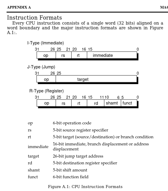
For the special cases where the highest 6 bits are not enough to determine the instruction, the opcodes are still pretty regular. For example, if the highest 6 bits are all 0, then the lowest 6 bits are guaranteed to be enough to determine the instruction. This makes MIPS opcodes very simple to decode compared to a lot of other CPU architectures.
Delays
And now for the most annoying part of emulating the R3000: branch delays and load delays.
Branch
Branch delays were also present in the Super FX GSU, and they work pretty much the same way here for the same reasons. When a branch is taken, the CPU has already started to decode and execute the instruction immediately following the branch, and the hardware designers decided to have the CPU finish executing that instruction instead of canceling it (which could be expensive).
An emulator must emulate branch delays because software will often put a useful instruction in the branch delay slot, knowing that it will always be executed even if the branch is taken. I handle this with one additional field:
|
|
When a jump or branch instruction is executed, the instruction implementation sets delayed_branch = Some(address) instead of directly writing to the program counter. Opcode execution looks roughly like this:
|
|
That’s not too bad, but unfortunately the R3000 also has this awful thing known as load delay.
Load
Due to how the R3000 pipelines instruction execution, when a load instruction reads data from memory, that data is not available to the very next instruction. I think it’s easier to explain this with an example:
|
|
The andi r10, r9, 0x007F instruction will use whatever value was previously in R9 instead of using the value that was just loaded from memory, because the value from memory has not yet been persisted to the register file. The instruction after the andi will be able to see the newly loaded R9 value.
Software typically works around this by just sticking an effective no-op in between the load and the instruction that uses the data:
|
|
Load delay was pretty much universally condemned as a terrible thing to expose to software, not just because it’s annoying to deal with but also because it exposes hardware details that could change in later hardware revisions. Later MIPS revisions realized this and completely removed the concept of load delay, at least as far as it being visible to software.
Now, a PS1 emulator mostly does not need to emulate load delay, because not much depends on it. Software generally either sticks an unrelated instruction in the load delay slot or puts an effective no-op there, so the vast majority of software is not sensitive to load delay existing or not.
If you do emulate load delay, take care to handle the case where the instruction in a load delay slot writes to the same register as the immediately preceding load instruction! I think the write from the load delay slot should take priority, mainly because the BIOS boot code does not work correctly if you don’t do that. It executes jal instructions immediately following lw r31, ... instructions and it expects R31 to contain the return address from jal, not the word loaded from memory.
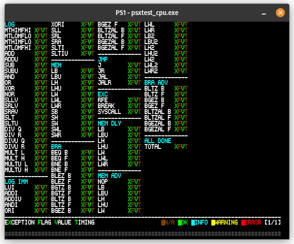
This is roughly how I do it, which passes psxtest_cpu.exe:
|
|
Load Word Left
One other annoying thing about emulating the R3000 is dealing with the partial word load/store instructions: LWL (Load Word Left), LWR (Load Word Right), SWL (Store Word Left), and SWR (Store Word Right). Unlike load delay, I’m sure these were useful for programmers and compilers, they’re just tricky to emulate.
The basic idea behind all four of these instructions is that they operate on full 32-bit words, but they may only modify some of the bytes in that word. Here’s the hardware manual attempting to explain just what exactly LWL does:
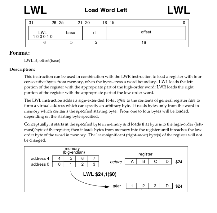
If you think you’ve made sense of that, well, the PS1’s CPU is exclusively little-endian which adds another layer of fun to deciphering this. “Left” still means read the least significant bytes of the source into the high bytes of the destination, and “right” still means read the most significant bytes of the source into the low bytes of the destination, but you have to account for the fact that little-endian changes which addresses map to which bytes within a word compared to the big-endian example.
Thankfully there are test programs for this so that you don’t have to guess whether you’ve emulated these instructions correctly, such as Amidog’s psxtest_cpu.exe.
One quirk with LWL and LWR is that they bypass load delay when reading the target register. According to documentation, these instructions have special circuitry in the processor that allows them to read an in-flight load to the target register so that software can execute consecutive LWL and LWR instructions without needing to insert a no-op in between. Load delay does still apply to LWL and LWR themselves, so software does still need to insert a no-op before using the register after the final LWL/LWR instruction.
Here’s how I handle load delay in LWL/LWR, using the same Registers struct as above:
|
|
Coprocessors
The MIPS I ISA supports coprocessors which can be accessed using special coprocessor opcodes. The PS1 has two MIPS coprocessors:
- Coprocessor 0: System Control Processor
- Coprocessor 2: Geometry Transformation Engine (GTE)
The ISA also supports coprocessors numbered 1 and 3, but those slots are empty in the PS1. The ISA reserves coprocessor 1 for a potential floating-point unit and the PS1 doesn’t have one of those, hence the GTE being CP2 instead of CP1.
The GTE is a core part of the PS1’s 3D graphics pipeline, but I’m not going to cover it in detail here. It’s essentially a 3D math coprocessor that supports hardware-accelerated vector and matrix operations in fixed-point decimal.
The system control processor, or CP0, is much more important to discuss here because it’s a core part of how the CPU functions in general. At a high level, it’s responsible for everything related to exception processing.
Exceptions
An exception is anything that disrupts normal instruction execution: an interrupt, an address error (i.e. an unaligned memory access), a signed arithmetic overflow, a bus error (i.e. accessing an unmapped memory address), and a few other things. Software can also forcibly trigger an exception by executing a SYSCALL or BREAK instruction. The CPU handles all exception types (mostly) exactly the same way, relying on software to deal with figuring out how to process different types of exceptions.
CP0 has a few internal registers that are important for dealing with exceptions:
- SR (R12): Used to enable interrupts and to mask specific interrupt lines, among other things
- Cause (R13): Contains interrupt pending bits and an exception code indicating the type of the most recently triggered exception
- EPC (R14): Contains the address of the instruction that triggered the exception
- If the exception is an interrupt, EPC contains the address of the next instruction that would have been executed
- BadVaddr (R8): On address error exceptions, this register contains the address that triggered the exception
When an exception triggers, the CPU does the following:
- Store the current PC in the EPC register
- Unless the CPU is currently in a branch delay slot, in which case it will set EPC to (PC - 4) and also set a bit in Cause to indicate that the exception triggered in a branch delay slot. This is important to ensure that the exception handler will return to the correct location
- Store the exception code in the Cause register
- Disable interrupts, enable kernel mode, and push an “exception stack” in SR (records previous interrupts enabled and user/kernel mode bits)
- If the exception was an address error, store the problematic address in the BadVaddr register
- Jump to the exception vector:
$BFC00180if the Boot Exception Vectors (BEV) bit in SR is set, otherwise$80000080- BEV is set at boot, but the PS1 BIOS clears it very early on and leaves it cleared
That’s it! Software is responsible for deciding what to do with the exception after the CPU jumps to the exception vector. In the PS1’s memory map, the standard exception vector is near the start of main RAM and the boot exception vector is in BIOS ROM.
As far as how to interact with CP0 (and the GTE), the MIPS I ISA has a number of instructions specifically for interacting with coprocessors. They are:
- Instructions to load a coprocessor register from a CPU register or memory (MTCz, CTCz, LWCz)
- Instructions to store a coprocessor register to a CPU register or memory (MFCz, CFCz, SWCz)
- An instruction to execute a coprocessor command (COPz)
For CP0, the only supported command via COP0 is RFE (Restore From Exception), which simply pops the exception stack in the SR register.
Interrupts
Interrupts are mostly just a special case of exceptions as far as the CPU is concerned, but they do get a bit of special handling in CP0.
The R3000 has 8 different interrupt lines: 2 software interrupt lines and 6 hardware interrupt lines. Each line has a mask bit in the SR register and a pending bit in the Cause register. Software can write to all 8 of the mask bits but can only directly write to the 2 software pending bits, not the 6 hardware pending bits - these are (supposed to be) connected to external devices.
The PS1 only uses 1 of the hardware interrupt lines, which is set if any device is currently raising an interrupt (and is automatically cleared when no devices are raising an interrupt). Software exception handlers need to check the PS1’s I_STAT and I_MASK registers to determine which device(s) caused the interrupt.
An interrupt exception triggers whenever sr.interrupts_enabled && (sr.interrupt_mask & cause.interrupts_pending) != 0 is true. CP0’s hardware exception handling automatically disables interrupts so that interrupts cannot trigger repeatedly before the software’s exception handler can deal with them.
Memory Layout
The R3000 has a 32-bit address space that is split into 4 regions:
- $00000000-$7FFFFFFF: kuseg (2GB user memory)
- $80000000-$9FFFFFFF: kseg0 (512MB cached kernel memory)
- $A0000000-$BFFFFFFF: kseg1 (512MB uncached kernel memory)
- $C0000000-$FFFFFFFF: kseg2 (1GB virtual memory)
In the PS1, kuseg/kseg0/kseg1 are all essentially mirrors of the same 29-bit address space with different attributes. kseg2 is entirely unmapped except for $FFFE0130 which maps to a CPU cache control register. Only the first 512MB of kuseg is mapped - accessing an address in $20000000-$7FFFFFFF will trigger a bus error exception.
kuseg is a userspace view of memory (which is always cached), kseg0 is a cached kernel view of memory, and kseg1 is an uncached kernel view of memory. PS1 games generally don’t disable kernel mode, so there’s not much practical difference between using kuseg and using kseg0. Accessing kseg0 or kseg1 outside of kernel mode will trigger a bus error exception. Accessing any kseg2 address other than $FFFE0130 will also trigger a bus error exception.
The distinction between cached and uncached memory matters in two ways: the instruction cache, and the write queue. (Also the data cache, but the PS1 CPU doesn’t really have a data cache.) Memory accesses in kuseg and kseg0 use both I-cache and the write queue, while memory accesses in kseg1 use neither.
Instruction Cache
The R3000 has an instruction cache that it uses whenever it is executing code out of kuseg or kseg0. I-cache is very important for performance - on the PS1, an instruction that executes out of I-cache and doesn’t access the bus can finish in a single cycle (from software’s perspective), while an uncached instruction that executes out of RAM usually takes 6 cycles.
The PS1 has 4KB of I-cache that is split into 4-word cache lines, indexed using the lower bits of the address. Each cache entry is tagged with the higher address bits to ensure that an opcode read from a different address will never fetch wrong data from that cache entry. (Although opcode reads can still fetch stale data from I-cache if the underlying memory has been modified!)
The I-cache is populated automatically when executing code out of kuseg or kseg0. When the CPU fetches an opcode that misses in I-cache, it will automatically populate the cache line after fetching the opcode from memory. Software generally only needs to be conscious of the I-cache when modifying existing code in RAM, in which case the software will probably want to invalidate the entire cache before executing any of the new code in order to guarantee that no stale opcodes are read from cache.
Software performs cache invalidation by invoking a BIOS kernel function, flushCache(). As far as I can tell, the kernel implements this function by setting the “isolate cache” bit in the CP0 SR register and then writing at least one byte to every cache line. The kernel never sets the SR “swap caches” bit described in the R3000 documentation, and it’s possible that this bit doesn’t even do anything in the PS1 CPU. It likely isn’t necessary since the PS1 CPU doesn’t have a true data cache.
While a lot of games will work just fine without emulating I-cache (I don’t yet), there are apparently some games that require I-cache emulation to function correctly due to relying on I-cache returning stale data if the underlying memory value has changed.
Write Queue
Writes to memory addresses in kuseg and kseg0 are performed asynchronously so that software can continue to execute while the hardware persists the write to memory. The R3000 has a 4-word queue for writes to cached memory addresses, and the CPU will only stall on writes if the write queue is full.
Reading from a kuseg/kseg0 address that has a pending write in the write queue will stall the CPU until the write is applied, to guarantee that the CPU does not read stale data. Additionally, reading from any uncached address (i.e. kseg1) will stall the CPU until the entire write queue is flushed.
Timings
Every R3000 instruction takes 1 cycle from software’s perspective if the opcode is read from I-cache and the instruction does not access memory. The only notable exceptions are the multiplication/division instructions and certain coprocessor instructions.
Multiplication/division operations execute asynchronously starting when the CPU executes the MUL/MULU/DIV/DIVU opcode. The result is automatically written to the HI and LO registers once the operation completes, and the CPU will stall if it accesses HI or LO while a multiplication/division operation is still in-progress. Multiplication takes between 6 and 13 cycles depending on the operand values, and division always takes 36 cycles.
Executing a COP2 command (GTE) will stall the CPU until the GTE operation completes. GTE operations can take up to 44 cycles depending on which command is executed.
Because the PS1 CPU doesn’t have a data cache, reads from memory will always stall the CPU during the memory access. Reading from main RAM usually takes 5 cycles and a 32-bit read from BIOS ROM usually takes 24 cycles (not including the instruction execution cycle, so 6 cycles / 25 cycles total). Memory reads may also wait for a write queue flush - reads from uncached memory always wait for the write queue to empty, and reads from cached memory will wait if there is an in-progress write to the memory address being read.
Writes to uncached memory will stall the CPU until the write completes, but writes to cached memory will not stall as long as there is room in the write queue.
Now, for getting a new emulator started, you can ignore a lot of that and just have every instruction take 2 cycles with no memory access delays or even write queue emulation. This isn’t remotely accurate but a decent number of games will work. (1 cycle/instruction causes a lot of games to run too fast, and 3 cycles/instruction starts to cause problems from the CPU running too slowly.) Some games do require semi-accurate timing though - nothing depends on instruction-by-instruction timing accuracy as far as I know, but some games do depend on aggregate timing of chunks of code being roughly correct.
psxtest_cpu.exe
My CPU implementation fully passes Amidog’s psxtest_cpu.exe:
Aside from the load delay trickery I mentioned above, there are two other things to keep in mind.
Unofficial Branch Opcodes
The BRA ADV tests depend on undocumented branch opcodes. This isn’t terribly difficult to emulate - there aren’t any new instructions to implement, only undocumented opcode mappings.
If the highest 6 bits of the opcode are $01 then the instruction is always one of BLTZ, BGEZ, BLTZAL, or BGEZAL, determined by opcode bits 16-20. The official mappings are:
- $00: BLTZ
- $01: BGEZ
- $10: BLTZAL
- $11: BGEZAL
The actual mappings are:
- $10: BLTZAL
- $11: BGEZAL
- All other values: BLTZ if opcode bit 16 is clear (0bxxxx0), BGEZ if opcode bit 16 is set (0bxxxx1)
Division by Zero
Since division operations execute asynchronously, a divide by zero operation sets specific values in HI and LO instead of triggering an exception. Amidog’s site describes the behavior here. To summarize, this is how DIV and DIVU behave when the divisor is 0:
- Remainder is always set to the dividend
- DIV with a non-negative dividend and DIVU set the quotient to $FFFFFFFF (-1)
- DIV with a negative dividend sets the quotient to $00000001 (+1)
Next
I think the next post will be a short one covering how an emulator can implement PS1 EXE sideloading, which is necessary in order to run test programs like the aforementioned psxtest_cpu.exe.