This post will overview what is required for a PS1 emulator to get any graphical output from test programs. PS1 test programs are typically designed such that they don’t use most (if any) of the GPU’s rasterization capabilities - they’ll either render their output pixel-by-pixel, or they’ll just copy the frame directly into VRAM using the CPU.
Frame Buffers and VRAM
First, a high-level overview of how the GPU works. It’s very different from the graphics processors in earlier consoles, which typically drew graphics pixel-by-pixel in real time based on current register and VRAM contents. Pixel colors were beamed out to the screen almost immediately after being drawn.
The PS1 GPU displays graphics from a frame buffer that is stored in the GPU’s 1MB of VRAM. Instead of drawing graphics to the screen in real time, the GPU draws graphics into a frame buffer, and display simply beams out pixel colors from the frame buffer. Games typically maintain two frame buffers in VRAM: a display buffer that is being actively displayed by the GPU, and a draw buffer where the game is drawing the next frame (in parallel to the GPU displaying the current frame). When a new frame is ready to display, the game waits until the GPU finishes displaying the current frame and then swaps the two frame buffer pointers. This technique is called double buffering and it is extremely common in graphics even today.
The GPU supports a number of different frame buffer resolutions. The horizontal resolution can be 256px, 320px, 368px, 512px, or 640px. The vertical resolution can be 240px or 480px, although 480px is only supported in interlaced display mode (which looks rather bad on actual hardware). 320x240 is the most common resolution but many games use other resolutions; for example, the Crash and Spyro games mainly use 512x240. Final Fantasy VII mostly uses 320x240, but it uses 368x240 for its menus.
H640px and V480px were not commonly used, but some games (and the BIOS shell) use 640x480 to display high-resolution splash screens and/or menus. These tend to not look great on actual hardware due to the interlaced display, but an emulator can make them look quite sharp.
The frame buffer color depth can be configured to either 15-bit (32,768 colors) or 24-bit (16,777,216 colors). 24-bit color looks much better, but the GPU’s draw commands can only output in 15-bit color, so 24-bit is really only used for static images and movies where the CPU (or DMA) can copy the 24-bit graphical data directly into VRAM.
For a new PS1 emulator, it’s a bit simpler to display the entire contents of VRAM rather than trying to only display the current frame buffer. This is also helpful for debugging because you can see data being written to the non-displayed parts of VRAM, such as texture data.
VRAM is logically arranged as a 2D grid of 512 rows, with each row containing 2KB of data. The number of data points within a row depends on the type of data. A single pixel in 15-bit color takes 2 bytes, so if you assume 15-bit color then VRAM can be interpreted as a 1024x512 grid of pixels.
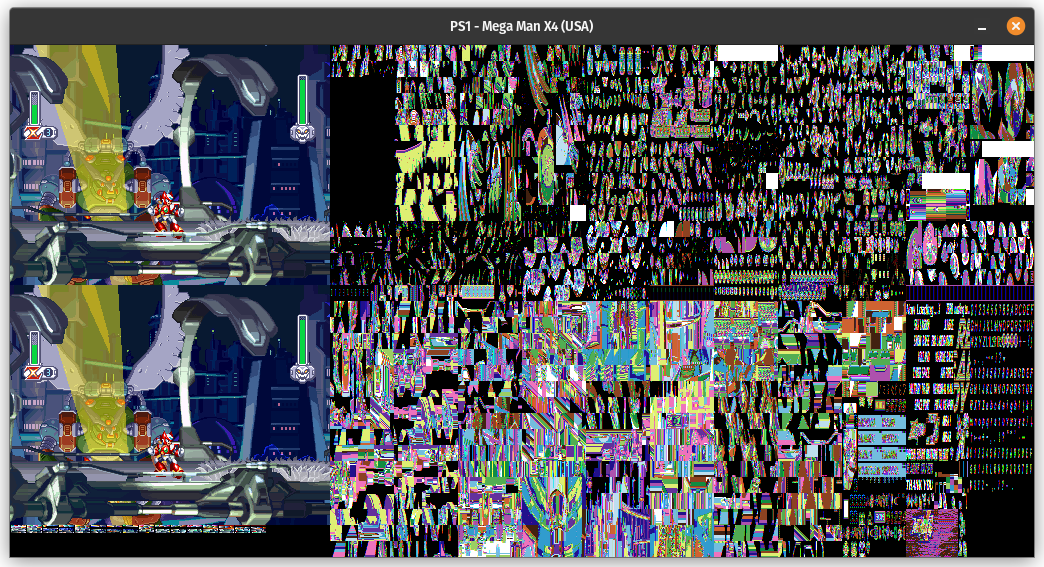
Here is what a VRAM view in Mega Man X4 looks like:

You can see the two 320x240 frame buffers at the left side of VRAM. Everything to the right of that is texture data, which looks distorted in this view because textures are typically stored in a compressed format: instead of storing raw 15-bit colors, the texture contains indices into a CLUT (color lookup table) with each index being either 4-bit (16-color texture) or 8-bit (256-color texture). The seemingly random color strips under the frame buffers are these CLUTs.
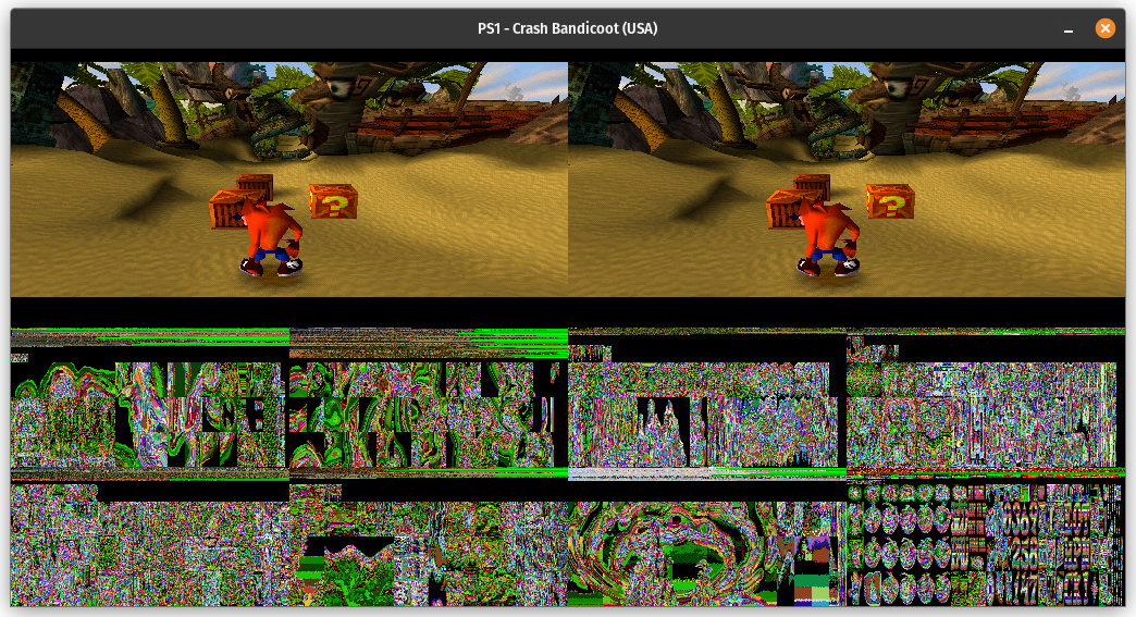
For an example of a game with a different VRAM layout, here’s Crash Bandicoot:

You can see that it puts its two 512x240 frame buffers at the top of VRAM, with textures and CLUTs intermixed below.
The GPU itself does not care how data is laid out in VRAM. Software tells it where the (display) frame buffer is located, software tells it where to write draw output, and software tells it where a particular texture/CLUT is located when it wants the GPU to rasterize a texture-mapped polygon or rectangle.
If you have a reference to VRAM as a byte array, generating a VRAM display like this is fairly simple:
|
|
In Rust I like to use bytemuck for the frame buffer so that I can update it as an array of structs but present it to the rendering code as a byte array, without needing to copy the memory. With the bytemuck::Pod trait derived (which requires bytemuck::Zeroable) and with a #[repr(C)] up top, a simple bytemuck::cast_slice(&frame_buffer) is all it takes to present a &[Color] as a byte array of RGBA8888 colors. If you wanted BGRA8888 or ARGB8888 or some other format instead, you could simply change the field order in the struct definition. repr(C) prevents the compiler from reordering the fields (and derive(bytemuck::Pod) enforces that the type is repr(C), among other restrictions).
I/O Ports
First, I’ll link the psx-spx page on the GPU, which was my primary source when I started working on the GPU.
The CPU interacts with the GPU entirely through four 32-bit I/O ports, two read ports and two write ports:
- Read $1F801810: GPUREAD (GPU data port)
- Read $1F801814: GPUSTAT (GPU status register)
- Write $1F801810: GP0 command port (also used as a VRAM data port with certain commands)
- Write $1F801814: GP1 command port
GPU DMA also uses these ports, specifically $1F801810. CPU-to-GPU DMA writes all words to $1F801810, and GPU-to-CPU DMA reads all words from $1F801810.
GPUREAD is mainly used for reading VRAM, but some commands also send responses that the CPU can read through GPUREAD.
Commands
Generally speaking, GP0 commands are draw-related while GP1 commands are display-related. In both cases the highest 8 bits are enough to uniquely determine the type of command. Most GP0 commands require additional parameter words after the first word, which are also sent through the GP0 command port.
Most GP0 command words go into a command FIFO rather than being executed immediately, but emulating the FIFO is not necessary for the majority of software. A lot of software will work fine if GPU commands finish instantly from software’s perspective.
For GP0 commands, only the highest 3 bits are needed to identify the most common commands:
- 001 (1): Draw polygon
- 010 (2): Draw line
- 011 (3): Draw rectangle
- 100 (4): VRAM-to-VRAM copy
- 101 (5): Begin CPU-to-VRAM copy
- 110 (6): Begin VRAM-to-CPU copy
- 000 (0) or 111 (7): Need to look at the rest of the highest 8 bits
- $00: No-op (sometimes used as filler in command lists)
- $01: Flush texture cache
- $02: VRAM fill
- $1F: Set GPU IRQ flag (almost never used)
- $E1: Set texture page and draw mode settings
- $E2: Set texture window mask/offset
- $E3: Set drawing area top-left coordinates
- $E4: Set drawing area bottom-right coordinates
- $E5: Set drawing offset
- $E6: Set mask bit settings
GP1 commands, looking at the highest 8 bits:
- $00: Reset GPU
- $01: Reset GP0 command state
- $02: Acknowledge GPU IRQ (almost never used)
- $03: Enable/disable display
- $04: Set GPU DMA direction (mainly just affects some DMA-related bits in GPUSTAT)
- $05: Set display area top-left coordinates
- $06: Set horizontal display range (in GPU clock units; $260 / 608 is roughly the left edge of the screen)
- $07: Set vertical display range (in scanline units; screen top/bottom values vary between NTSC and PAL modes)
- $08: Set display mode (resolution, color depth, interlacing, NTSC vs. PAL)
- $10: Read GPU register
Now, if you just want graphical output from psxtest_cpu.exe, you don’t need to implement most of these commands right away.
Setting Up
First, the BIOS does not access the GPU ports at all before it begins to execute the shell, at which point the emulator can sideload the EXE.
psxtest_cpu.exe begins by resetting the GPU to get it into a known state:
GP1: $00000000 // Reset GPU
After this it reads GPUSTAT a few times, waiting for specific bits to get set. It first waits for bit 26 to get set, then bit 28, then bit 26 again, then bit 28 again. Bit 26 is the “ready to receive GP0 command word” bit and bit 28 is the “ready to receive DMA block” bit. Initially an emulator can hardcode both of these to 1 to indicate that it’s always ready to receive GP0 commands, whether directly from the CPU or via DMA.
After those checks, it starts sending more commands:
GP1: $01000000  // Reset GP0 command state
GP0: $A0000000  // Begin CPU-to-VRAM copy; expects 2 parameter words followed by some number of data words
GP0: $01FF0000  //   1st parameter: Set VRAM destination coordinates to (0, 511)
GP0: $00010002  //   2nd parameter: Set copy size to 1 row, 2 halfwords
GP0: $FFFFFFFF  //   Data word: 2 halfwords that are both $FFFF
So, this ultimately sets both (0, 511) and (1, 511) to $FFFF.
The program waits for GPUSTAT bits 26 and 28 again, then sends an opposite sequence of commands:
GP1: $01000000  // Reset GP0 command state
GP0: $C0000000  // Begin VRAM-to-CPU copy; expects 2 parameter words, then CPU can read data via GPUREAD
GP0: $01FF0000  //   1st parameter: Set VRAM source coordinates to (0, 511)
GP0: $00010002  //   2nd parameter: Set copy size to 1 row, 2 halfwords
It then reads GPUSTAT to wait for bit 27 to get set, which is the “ready to send VRAM data to CPU” bit. This bit normally gets set after receiving the second VRAM-to-CPU parameter word and then gets cleared after the CPU has read all data words.
After that the CPU reads the data word via GPUREAD, and it gets back the $FFFFFFFF that it previously wrote, although it doesn’t do anything with the result.
Finally, it sends one more command, this one a query:
GP1: $10000007 // Read GPU register 7; CPU can read response through GPUREAD
This command’s behavior seems to vary based on GPU version - there were apparently several different GPU versions used in different hardware revisions. On the earliest GPU versions this command does nothing and leaves the existing GPUREAD contents unchanged, so in this specific case the next GPUREAD read will still return $FFFFFFFF. On later GPU versions this command returns the GPU version number, which will be $00000001 or $00000002. I just hardcode my GPU version to 2.
The program waits for GPUSTAT bits 26 and 28 one more time, and then it reads GPUREAD and checks what it got back. Apparently all this was just to detect the GPU version! It doesn’t touch the GPU again until after it’s finished running all of the CPU tests.
Command State Machine
psxtest_cpu.exe doesn’t use the CPU-to-VRAM or VRAM-to-CPU copy commands for actually rendering graphical output, but they’re two of the easier GP0 commands to implement. Let’s look at CPU-to-VRAM.
The emulator knows as soon it sees the $A0000000 write to GP0 that it should begin executing a CPU-to-VRAM copy, but then it needs to wait for the CPU to write the 2 parameter words before it can initialize the copy, and then it needs to wait for the CPU to write each data word individually before it can actually do the copy. To me, this screams state machine.
I think it’s simpler to avoid processing the parameters until the CPU has sent all of them. Some of the GP0 commands have a variable number of parameters, but in every case the first command word is enough to know how many parameters there will be.
So, we can set things up like this:
|
|
Upon receiving a GP0 write, we look at the current state to determine what to do with it:
|
|
Since this command expects data words to be sent through GP0 after all parameters are sent, we’ll need another state for that:
|
|
Initialization is pretty straightforward once both parameters have been passed:
|
|
When the CPU sends a data word, persist those 2 halfwords to VRAM:
|
|
That ought to work.
VRAM-to-CPU copy works basically the same way, only in the reverse direction and with the CPU reading from GPUREAD instead of writing to the GP0 port.
You may not want to represent the command states exactly this way, especially since there are a number of different commands that expect to receive some number of parameters before executing and those all function basically the same way: store parameter, then execute command if it was the last parameter.
You could also queue up the GP0 writes and wait to actually persist anything to VRAM until all words have been written, though note that the CPU can technically end a transfer partway by sending a GP1($00) or (probably) a GP1($01) command. There’s not a good reason for software to do that though.
Pixels Are Just Tiny Rectangles
Okay, now for the part where psxtest_cpu.exe starts to actually render the test result output.
It starts out by resetting the GPU just like it did at the start, then it sends some GP0 commands to properly initialize drawing:
GP1: $00000000  // Reset GPU
GP1: $01000000  // Reset GP0 command state
GP0: $E1000400  // Clear texture page settings, allow drawing into display area, disable dithering
GP0: $E2000000  // Clear texture window mask/offset
GP0: $E3000000  // Set drawing area top-left coordinates to (0, 0)
GP0: $E407FFFF  // Set drawing area bottom-right coordinates to (1023, 511)
GP0: $E5000000  // Set drawing offset to (0, 0)
GP0: $E6000000  // Clear mask bit settings
Notably, it sets the drawing area to the rectangle ranging from (0, 0) to (1023, 511) which is the entirety of VRAM. The rasterizer will automatically clip any pixels that are drawn outside of the drawing area, which is normally useful to prevent it from drawing any pixels outside of the draw buffer.
Finally, it starts sending draw commands!
GP1: $01000000  // Reset GP0 command state
GP0: $68000000  // Draw rectangle; size of 1x1, untextured, semi-transparency disabled, color of R=0 G=0 B=0
GP0: $00000000  //   1st (and only) parameter: Set rectangle top-left coordinates to (0, 0)
This is drawing a solid black 1x1 rectangle starting at (0, 0) in VRAM. In other words, it’s painting a single pixel black, specifically the top-left corner of VRAM.
psxtest_cpu.exe renders its graphical output like this, by sending a ton of individual “draw 1x1 rectangle” commands. An actual game would never do this because it’s horrendously slow compared to drawing text using textured rectangles, but doing it this way definitely makes it easier for a new emulator to get graphical output from this test program!
Here’s a slightly more interesting command, since it has an actual color and coordinates:
GP0: $68004080  // Draw rectangle; size of 1x1, untextured, semi-transparency disabled, color of R=128 G=64 B=0
GP0: $00040090  //   Parameter: Set rectangle top-left coordinates to (144, 4)
This command paints the pixel at (144, 4) in VRAM a shade of brown.
For an untextured rectangle, the color is embedded in the command word. Color components are 8-bit (0-255), although the lowest 3 bits get dropped since draw commands can only output in 15-bit (RGB555) and not 24-bit (RGB888). You could theoretically round each color component to the nearest 5-bit value instead of truncating, but actual hardware appears to truncate.
The number of parameters for the draw rectangle command varies based on whether the rectangle is textured and whether the size is “variable” instead of using one of the fixed sizes. There is always at least 1 parameter which is the location of the top-left corner of the rectangle, specified in VRAM pixel coordinates. For a 1x1 rectangle, the coordinates are simply the pixel to paint.
Ignoring the state machine part of things (and ignoring draw settings), if you assume that draw rectangle commands will always be for 1x1 untextured rectangles and will never have semi-transparency enabled, this command is not too bad to implement:
|
|
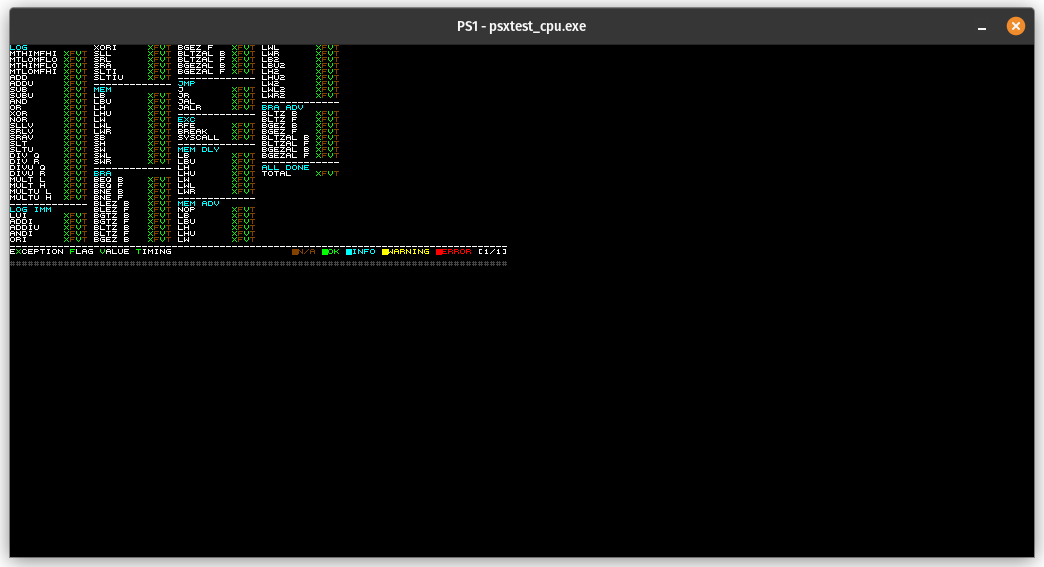
After wiring everything up, the test program renders pixels!

It looks rather stretched horizontally because it’s using a 512x240 frame buffer, which normally the GPU would squish into the correct aspect ratio while displaying. Not a big deal for just getting test output though.
Render…When?
One rather important thing that I haven’t mentioned yet is when to have the emulator render a frame.
Games typically sync to a combination of the VBlank interrupt and the hardware timers, but test programs generally don’t care about those - they run their tests, draw the results, and then idle forever.
The absolute simplest solution is to render purely based on CPU cycle count. The CPU clock speed is 33.8688 MHz. If you assume exactly 60 frames per second (which is not precise but never mind that), that means that the GPU should display one frame every 33,868,800/60 = 564,480 CPU cycles. Just render VRAM once every 564,480 CPU cycles and you’ll at least be able to get graphical output from test programs.
Once you get around to implementing interrupts, you can also generate the VBlank interrupt at the same time that you render, which is actually not really wrong! Games often use the VBlank interrupt as the signal to swap the display frame buffer and the draw frame buffer, knowing that the GPU generates the VBlank interrupt right when it finishes displaying a frame.
GPU Tests
I’m not going to cover these in detail (at least not in this post), but the PeterLemon/PSX repo has some test programs that are really helpful for getting a new GPU implementation properly started beyond drawing 1x1 untextured rectangles.
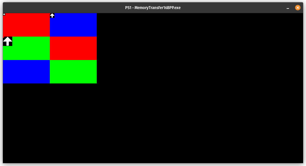
As an example, here’s the test under GPU/16BPP/MemoryTransfer/ which tests VRAM fill, VRAM-to-VRAM copy, CPU-to-VRAM copy, and VRAM-to-CPU copy:

Each test comes with a sample image that shows what the graphical output is supposed to look like.