This is maybe the start of a series of posts on games/software that exposed bugs in one of my emulators, depending on how many I find interesting enough to write about. In most cases I think the interesting part is usually the game behavior that triggered the bug rather than the bug itself.
There’s no groundbreaking research here - this is just a writeup on an issue that I personally encountered, that other more robust emulators solved many years ago.
The game in question is Kishin Douji Zenki: Tenchi Meidou for the Super Famicom, the last of five licensed games based on the obscure 90s manga/anime series Zenki.
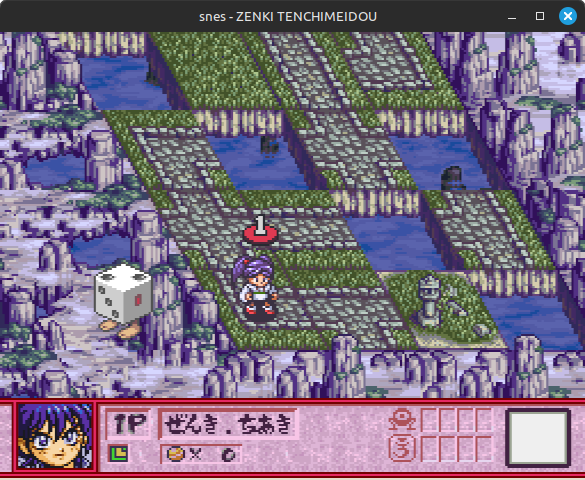
This seems to be some sort of virtual board game with a card-based combat system for fighting enemies. It’s fairly unplayable if you can’t read Japanese, which I cannot.
The Problem
The problem was very obvious: the game failed to boot. It hung forever at a black screen without ever displaying any graphics.
From my experience, a game failing to boot is almost always caused by one of two things: Either the game is stuck in an infinite loop waiting for something that will never happen, or some bug caused program flow to go completely off the rails (e.g. jumping to a non-code memory address). It is generally pretty easy to tell which happened by looking at the tail end of disassembly trace logs, though diagnosing the root cause(s) can be very involved.
Well, let’s see what we’ve got here:
da:03d4    lda #$10
da:03d6    sta $2141
da:03d9    lda $2140
da:03dc    cmp $2140
da:03df    bne -8      ; $03d9
da:03e1    cmp #$aa
da:03e3    bne -17     ; $03d4
da:03d4    lda #$10
da:03d6    sta $2141
da:03d9    lda $2140
da:03dc    cmp $2140
da:03df    bne -8      ; $03d9
da:03e1    cmp #$aa
da:03e3    bne -17     ; $03d4
da:03d4    lda #$10
...
65816 disassembly logs
Yep, that’s a loop alright.
If you’ve ever worked on an SNES emulator, or even SNES homebrew software, you know that seeing a seemingly-infinite loop polling any of addresses $2140-$2143 is a very bad sign.
Background: The SNES APU
The SNES APU (audio processing unit) is its own self-contained subsystem with a few different components.
Very importantly, the main SNES CPU (the 65816) cannot interface with the audio playback hardware directly. Instead, the APU has its own embedded fully programmable CPU for driving the playback hardware.
This embedded CPU is a Sony SPC700, an 8-bit CPU designed by Ken Kutaragi (yes, that Ken Kutaragi) alongside the rest of the SNES audio hardware. SPC700 is based on the 6502, though with its own proprietary extensions in the form of new instructions and addressing modes. Unlike the 65816, the SPC700 makes enough breaking changes to the 6502 ISA that it is not compatible with 6502 software - it’s its own unique 6502 variant.
The 65816 and the SPC700 can communicate only through a set of eight 8-bit communication ports: four one-way ports from the 65816 to the SPC700, and four one-way ports in the opposite direction. All communication and data transfer must go through these communication ports - there is no other shared memory (or any shared hardware) accessible to both CPUs.
On the 65816 side, these communication ports are mapped to $2140-$2143 in memory banks $00-$3F and $80-$BF. Reads from these addresses access the SPC700-to-65816 ports, and writes access the 65816-to-SPC700 ports.
When a game hangs with the 65816 infinitely polling the APU communication ports, that usually indicates some sort of desync between the 65816 main program and the SPC700 audio driver. These issues can be quite painful to debug.
One potential cause of desync issues is that a number of games have very fragile 65816/SPC700 communication code that is full of race conditions but happens to work on actual hardware due to very precise timings of the processors involved. (Spoilers: This game is one of those.)
Disassembly
Before looking at what the SPC700 is doing here, let’s clean up that 65816 disassembly a bit to make it clearer what it’s doing:
|
|
65816 loop
It writes 0x10 to APU port 1 (communication to SPC700), then it reads from APU port 0 (communication from SPC700) and loops if it read any value other than 0xAA. Simple enough.
lda $214x followed by cmp $214x and bne is a very common pattern for reading from the APU ports. One CPU can theoretically read an undefined value if it reads from the port at the exact same time that the other CPU writes to it, so the double read is a check to ensure that the value is stable. (It’s been observed that the 65816 will read the logical OR of the old and new values if it reads a port while the SPC700 writes to it, but I don’t think the exact timing of this behavior is well-understood.)
Moving on, let’s see what the SPC700 is doing while the 65816 is stuck here.
Sony created their own instruction names and assembly syntax for SPC700, but I’m going to use 6502-style names and syntax here to make this easier to read next to the 65816 code:
0965    lda $1d
0967    ora #$30
0969    sta $f1
096b    nop
096c    lda $f4
096e    ora $f5
0970    ora $f6
0972    ora $f7
0974    bne -17    ; $0965
0965    lda $1d
0967    ora #$30
0969    sta $f1
096b    nop
096c    lda $f4
096e    ora $f5
0970    ora $f6
0972    ora $f7
0974    bne -17    ; $0965
0965    lda $1d
...
SPC700 disassembly logs
Yep, that is also definitely a loop.
The SPC700’s memory map is thankfully very simple. $00F0-$00FF are memory-mapped I/O registers, and all other addresses map to the APU’s 64 KB of audio RAM.
…Well, $FFC0-$FFFF maps to a program loader boot ROM at power-on, but most games’ audio drivers unmap the boot ROM so that those addresses map to RAM.
The game accesses 6 memory addresses in this loop: $001D is RAM, $00F1 is the APU control register (details just below), and $00F4-$00F7 are the APU communication ports (the other side of the 65816’s $2140-$2143).
The APU control register at $00F1 has 6 meaningful bits:
- Bits 0-2: APU timer 0-2 enabled
- Bit 4: Clear communication ports 0 and 1 (write 1 to clear)
- Bit 5: Clear communication ports 2 and 3 (write 1 to clear)
- Bit 7: Boot ROM mapped
“Clearing” the communication ports means resetting the values of the 65816-to-SPC700 ports to 0. These values are latched within the APU, and writing to $F1 with these bits set clears the latches. Setting these bits has no effect on the SPC700-to-65816 ports.
Cleaning up / commenting the disassembly from above:
|
|
SPC700 loop
It first loads a value from RAM that presumably holds the current APU control value, which needs to be stored in RAM somewhere because the control register is not readable. It ORs that value with 0x30 (sets bits 4 and 5) and then writes that new value to the control register. This will clear all 4 APU communication port latches.
After it clears the ports, it executes a NOP for some reason (timing purposes?), then it validates that all 4 communication ports read 0 after it tried to clear them. If any of them are non-zero, it loops and tries again.
This is a little odd (does it not trust that the clear bits work reliably?), but maybe reasonable enough? At least, if you ignore what the 65816 is doing in parallel.
Copying both disassemblies from above so that they’re right next to each other:
|
|
65816 loop
|
|
SPC700 loop
The 65816 is repeatedly writing 0x10 to APU port 1 ($2141) while waiting for the SPC700 to write 0xAA to one of the ports in the other direction. The read branch will never trigger and the loop branch will always trigger because the SPC700 isn’t writing to any of the ports.
Meanwhile, the SPC700 is stuck a loop where it clears all 4 APU ports and then validates that they were cleared, but the validation always fails because APU port 1 ($F5) always holds 0x10 by the time the SPC700 reads from it.
This looks like a livelock!
The 65816 has both NMI and IRQ interrupts disabled in the SNES NMITIMEN register here, and the SNES doesn’t even wire up any of the SPC700’s interrupt lines, so no interrupts are ever going to trigger during these loops.
The only possible way for the game to break out of this is if enough time passes between 65816 sta $2141 instructions that the SPC700 can at some point get a 0 back from the ora $f5 read. I was able to validate this by artificially slowing down the 65816 just a little bit and voila, the game boots and seems to be fully playable:
Why doesn’t it work without the artificial slowdown? What’s the real problem here?
Inter-CPU Timing
From interleaved execution trace logs, I can see that the game is very close to breaking out of this livelock. The 65816 sta $2141 write changing the port value from 0x00 to 0x10 sometimes executes immediately before the SPC700 ora $f5 read. This implies that the timing is within a single SPC700 CPU cycle off from what the game seemingly depends on.
Let’s count some cycles to see just how close the game is to working, and to rule out obvious bugs like some instruction taking the wrong number of cycles.
The two CPUs are driven by different oscillators, so directly comparing cycle counts doesn’t make sense, but it’s possible to convert both CPUs’ cycle counts to wall clock times and compare those.
The 65816 is driven by the SNES master oscillator at roughly 21.477 MHz (NTSC), which it divides by 6 for a CPU clock speed of ~3.58 MHz. SNES 65816 timing in general can be quite complex due to memory wait states, but those thankfully aren’t a factor here - the game doesn’t access RAM in this loop, and it’s executing from cartridge ROM in a mode where the console won’t insert any wait states on cartridge reads (see the MEMSEL register). The console never inserts wait states on APU port accesses.
The APU has its own ~24.576 MHz oscillator that drives the SPC700 and the rest of the audio hardware, with the SPC700 specifically dividing it by 24 for a clock speed of 1.024 MHz. Measurements on actual hardware have shown that the APU oscillator often runs slightly faster than 24.576 MHz in practice (and that there’s variance between different consoles), but it’s not by enough to make a real difference here - it’s much less than a 1% difference in speed compared to 24.576 MHz.
Alright, first, the 65816 loop:
|
|
21 cycles total at 3.58 MHz (21.477 MHz / 6) for each iteration of the loop.
Next, the SPC700 loop:
|
|
27 cycles total at 1.024 MHz for each iteration of the loop, but the important part is really how many cycles elapse between the APU control write (sta $f1) and reading APU port 1 (ora $f5). The memory access occurs on the last cycle of each of these instructions, so there are 8 cycles between these two memory operations.
Converting these cycle counts to wall clock times, in seconds:
|
|
Yeah, based on this, the SPC700 is not even close to being able to read 0 from that port. That time difference is roughly equal to 7 65816 cycles or 2 SPC700 cycles:
|
|
There’s something missing because this doesn’t match the behavior I see in the emulator, where the 65816 sta $2141 write cycle sometimes executes immediately before the SPC700 ora $f5 read cycle.
Yes, this napkin math has a significant omission on the 65816 side: memory refresh delay. The SNES stalls the 65816 for 40 master clock cycles once per scanline, during which time it refreshes the console’s working RAM. The loop iterations that include a memory refresh are significantly longer:
|
|
That is much closer, but the 65816 loop is still slightly too fast for the SPC700 to ever read 0 from that port. However, note that the difference between the times is now much less than 1 clock cycle, for both CPUs:
|
|
A timing difference that small is very possible to deal with!
The Fix
There are a few ways to fix this that are not likely to break any other games.
One is to make SPC700 memory reads and writes occur at different times within the CPU clock cycle, with reads occurring slightly earlier than writes. This might be how actual hardware behaves, but it almost certainly depends on the specific hardware devices.
Making reads happen even a quarter-cycle earlier than writes is enough to fix this game. It might take many loop iterations, but eventually the timings between the two CPUs will line up such that the SPC700 will read 0 from port $F5 less than a quarter of a cycle before the 65816 writes 0x10 to it, and the game will break free of this livelock.
Adding sub-CPU-cycle timing for the SPC700 seemed a little complex to implement for me (and potentially a performance hit), so I tried something probably less accurate but simpler: whenever the SPC700 clears the communication port latches by writing to $F1 with bit 4 or 5 set, I discard all 65816 writes to the cleared ports until the next SPC700 cycle, which shortens the time between latch clear and $F5 read by 1 cycle. This fixes Zenki: Tenchi Meidou and doesn’t seem to cause any issues for other games that are extraordinarily sensitive to inter-CPU timing (e.g. Tales of Phantasia, Rendering Ranger R2).
To some extent this is a problem created by the emulator needing to serialize accesses to these communication ports in order to do something somewhat reasonable when both CPUs access one roughly simultaneously. Actual hardware doesn’t necessarily behave in such a consistent and predictable manner, particularly given that it’s known that the 65816 will get nonsense if it reads from a port exactly while the SPC700 writes to it. This game clearly works with whatever actual hardware does, though!
I do wonder about the NOP that the SPC700 executes right after it writes to the APU control register. Maybe there is some very small latency to clearing the latches in actual hardware, or maybe the game programmers just thought there was latency because their code had the 65816 constantly writing to one of the ports.
Prior Art
ares and its predecessors bsnes and higan have long been the most accurate SNES emulator(s), so after I mostly figured this out I was curious to see how they make this game work.
If I’m reading the SPC700 I/O code correctly (quite possible I am not), for $F4-$F7 reads the memory read occurs halfway through the SPC700 clock cycle, while other memory reads and all memory writes occur at the end of the SPC700 cycle. So, it makes reads occur a half-cycle earlier relative to writes, but only for the communication ports.
Coincidentally, per the commit message, this timing behavior was introduced (and presumably tested on actual hardware) specifically because of this very game!